nedoPC.org

Electronics hobbyists community established in 2002
Atom Feed | View unanswered posts | View active topics It is currently 27 Apr 2024 10:39


Reply to topic  [ 14 posts ] 
NANDputer 
Author Message
Online
Admin
User avatar

Joined: 08 Jan 2003 23:22
Posts: 22602
Location: Silicon Valley
Reply with quote
Image

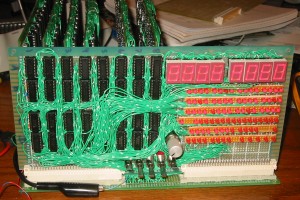
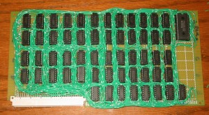
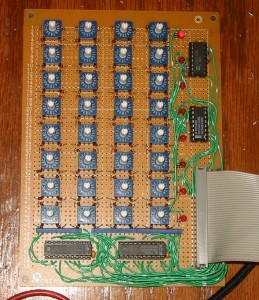
Уже пролетало, однако пусть будет ещё и тут:

http://blog.kevtris.org/?m=201303

Фигово конечно что нет ни схем, ни вообще какой-либо документации...

P.S. После опубликования на dangerousprototypes было в комментариях:

Quote:
Peter Camilleri says:
March 21, 2013 at 2:18 pm

Amazing but not without precidence though. I read that the Apollo Guidance and LEM computers were built out of dual 3 input NOR gates.!


Quote:
Matthew Hagerty says:
March 21, 2013 at 6:23 pm

Anyway, more related to this topic, I wonder if Kevin knows that the Cray-1 was built totally with NAND gates? They used three types of ICs in the whole computer, a NAND gate and two types of RAM. They did that because most ICs of the day were too slow. The NAND gate had sub 1ns time, which even for today is very fast.


P.P.S. Про Cray-1 чувак ошибся - он был на NOR построен, а не NAND...

_________________
:dj: https://mastodon.social/@Shaos


Last edited by Shaos on 13 May 2013 16:09, edited 1 time in total.


09 May 2013 19:16
Profile WWW
Online
Admin
User avatar

Joined: 08 Jan 2003 23:22
Posts: 22602
Location: Silicon Valley
Reply with quote
Post 
Я кстати иногда тыкаюсь в Logisim и строю всякое на NAND-ах чтобы проверить свои концепции - вчера например строил двухфазные D-триггеры и счётчики ;)

_________________
:dj: https://mastodon.social/@Shaos


09 May 2013 19:39
Profile WWW
Supreme God
User avatar

Joined: 21 Oct 2009 08:08
Posts: 7777
Location: Россия
Reply with quote
Post 
А RAM и ROM он всё-таки заюзал... что несколько неспортивно
с его стороны (ну, с точки зрения нищебродства) :wink: !

Image

Image

Ещё RAM - куда ни шло... а вот ROM - мог бы и диодной матрицей
обойтись...

_________________
iLavr


Last edited by Lavr on 14 May 2013 05:06, edited 1 time in total.


13 May 2013 15:06
Profile
Online
Admin
User avatar

Joined: 08 Jan 2003 23:22
Posts: 22602
Location: Silicon Valley
Reply with quote
Post 
Ну как же - вот у него ROM - на целых 8 слов :)

Image

_________________
:dj: https://mastodon.social/@Shaos


13 May 2013 16:08
Profile WWW
Supreme God
User avatar

Joined: 21 Oct 2009 08:08
Posts: 7777
Location: Россия
Reply with quote
Post 
Shaos wrote:
Ну как же - вот у него ROM - на целых 8 слов :)

Это П_О_К_А_З_У_Х_А! :wink: ROM - у него - ВОТ в верхнем правом углу! :o

Image

_________________
iLavr


13 May 2013 16:28
Profile
Online
Admin
User avatar

Joined: 08 Jan 2003 23:22
Posts: 22602
Location: Silicon Valley
Reply with quote
Post 
да может и 7400 напаяны тоже для показухи, а под пучками проводков спрятан PIC? ;)

чувак же схемы зажилил :)

_________________
:dj: https://mastodon.social/@Shaos


13 May 2013 16:35
Profile WWW
Supreme God
User avatar

Joined: 21 Oct 2009 08:08
Posts: 7777
Location: Россия
Reply with quote
Post 
Shaos wrote:
чувак же схемы зажилил :)

Да... неприятно как-то... как в поговорке:"поманил, да обманул"... :(
Но, впрочем, мы и без него фактически всё знаем.

И предъявы мои к ПЗУ - больше ирония. :wink:

Интересно, конечно же, взглянуть архитектуру, которой он придержался,
хотя бы в общих чертах...

Потому как сами узлы на NAND для нас тут не секрет, а вот подробности
"нищебродской" архитектуры всегда интерес вызывают.

_________________
iLavr


14 May 2013 04:48
Profile
Supreme God
User avatar

Joined: 21 Oct 2009 08:08
Posts: 7777
Location: Россия
Reply with quote
Post 
Shaos wrote:
Я кстати иногда тыкаюсь в Logisim и строю всякое на NAND-ах...


Потыкай его АЛУ на NAND-ах - вот и схемотехникой поинтересуемся...

http://blog.kevtris.org/blogfiles/NANDputer/nandalu.circ

_________________
iLavr


14 May 2013 14:16
Profile
Online
Admin
User avatar

Joined: 08 Jan 2003 23:22
Posts: 22602
Location: Silicon Valley
Reply with quote
Post 
Lavr wrote:
Shaos wrote:
Я кстати иногда тыкаюсь в Logisim и строю всякое на NAND-ах...


Потыкай его АЛУ на NAND-ах - вот и схемотехникой поинтересуемся...

http://blog.kevtris.org/blogfiles/NANDputer/nandalu.circ


o - а в блоге линков на это нету :)

_________________
:dj: https://mastodon.social/@Shaos


14 May 2013 15:12
Profile WWW
Supreme God
User avatar

Joined: 21 Oct 2009 08:08
Posts: 7777
Location: Россия
Reply with quote
Post 
Shaos wrote:
o - а в блоге линков на это нету :)

Но мы то с тобой выяснили - где его линки... :wink: Я там и пошарил...

Но думается мне - большую часть он в Квартусе строил.
У него большинство проектов в нем...

Картинку выложишь? А то я Логисим уволил...

_________________
iLavr


14 May 2013 15:26
Profile
Online
Admin
User avatar

Joined: 08 Jan 2003 23:22
Posts: 22602
Location: Silicon Valley
Reply with quote
Post 
Lavr wrote:
Картинку выложишь? А то я Логисим уволил...


А чего уволил? У меня всё ещё есть, хоть я джаву и похоронил уже :roll:

Image

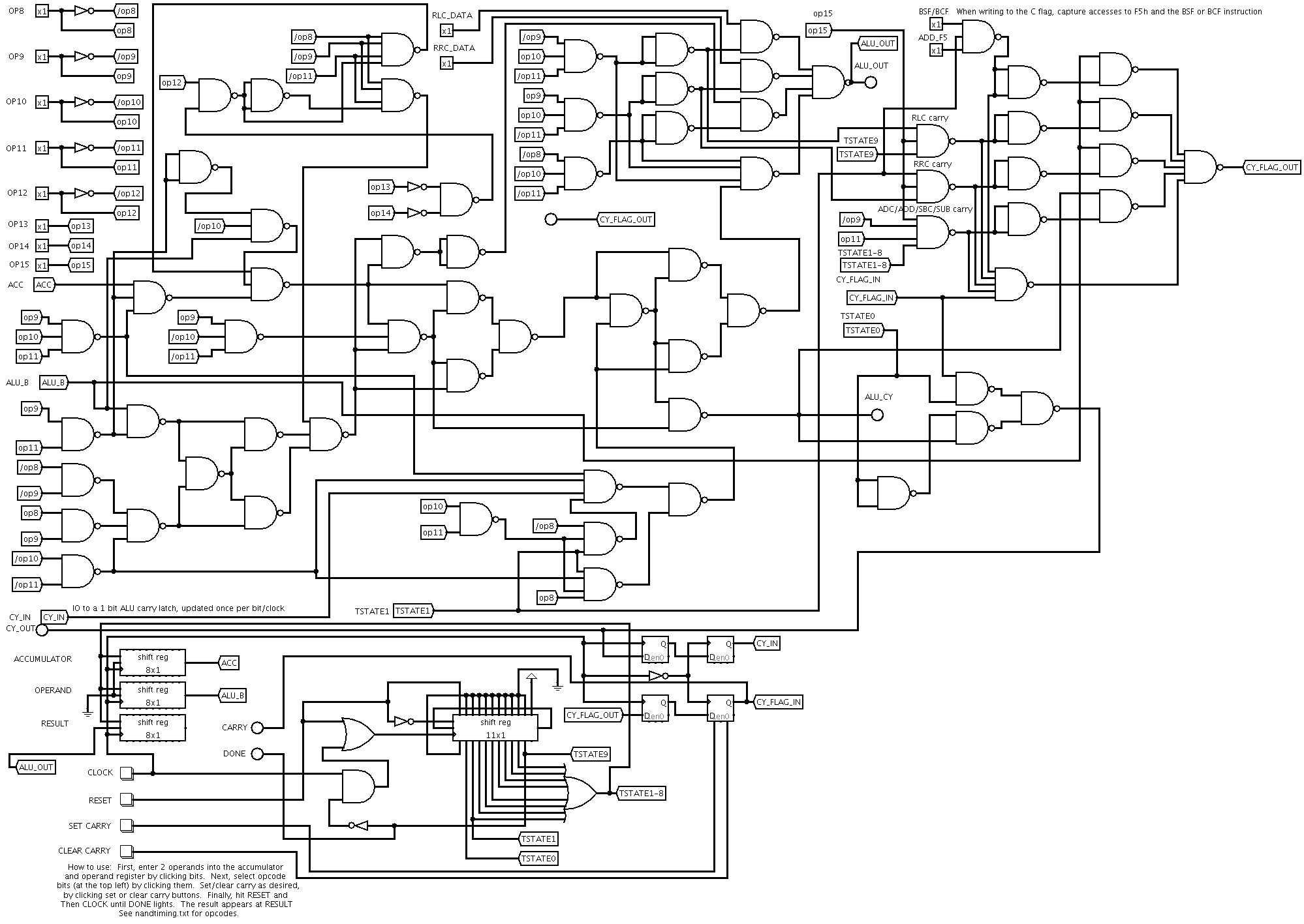
Кликабельно. У него кстати тут всякие нанды - не только двухногие.

_________________
:dj: https://mastodon.social/@Shaos


14 May 2013 17:49
Profile WWW
Supreme God
User avatar

Joined: 21 Oct 2009 08:08
Posts: 7777
Location: Россия
Reply with quote
Post 
Shaos wrote:
Lavr wrote:
Картинку выложишь? А то я Логисим уволил...

А чего уволил? У меня всё ещё есть, хоть я джаву и похоронил уже :roll:

Да что-то он ко двору не пришелся... я к другим двум пакетам привык, хоть вы их
и не пользуете.

За схему - благодарю!
А АЛУ-то 1-битное похоже?... :o я об этом подумал, еще когда страницу автора читал.

96 тактов у него на инструкцию, кажется? :wink: Ну а что ещё делать в 96 тактах?
Тут он даже EDUC-8 переплюнул по этому параметру!

_________________
iLavr


14 May 2013 18:09
Profile
Online
Admin
User avatar

Joined: 08 Jan 2003 23:22
Posts: 22602
Location: Silicon Valley
Reply with quote
Post 
Вот у него ещё текстики есть:
http://blog.kevtris.org/blogfiles/NANDp ... inouts.txt
http://blog.kevtris.org/blogfiles/NANDp ... timing.txt
Содержимое последнего файлика:
Code:
Data serialization:

T0    -     -      -     CARRY  CARRY  CARRY
T1   PC0   STK0   ROMD0  REGx0  RAM0   ROMD0  phi2: /RD high if needed
T2   PC1   STK1   ROMD1  REGx1  RAM1   ROMD1  ALU0
T3   PC2   STK2   ROMD2  REGx2  RAM2   ROMD2  ALU1
T4   PC3   STK3   ROMD3  REGx3  RAM3   ROMD3  ALU2
T5   PC4   STK4   ROMD4  REGx4  RAM4   ROMD4  ALU3
T6   PC5   STK5   ROMD5  REGx5  RAM5   ROMD5  ALU4
T7   PC6   STK6   ROMD6  REGx6  RAM6   ROMD6  ALU5
T8   PC7   STK7   ROMD7  REGx7  RAM7   ROMD7  ALU6
T9   PC8   STK8   ROMD8  CARRY  CARRY  CARRY  ALU7
T10  PC9   STK9   ROMD9   -      -      -     update RAM latch, if needed
T11  PC10  STK10  ROMD10  -      -      -     phi1: /WR low if needed
T12  PC11  STK11  ROMD11  -      -      -     phi2: /WR high if needed
T13   -     -      -      -      -
T14   -     -      -      -      -
T15   -     -      -      -      -      -     phi1: /RD low if needed


PC operations:

   ph0       ph1             ph2
0            stk 2->3        stk 1->2    (pushing)
1            PC->stk 1       latch PC0
2                            latch PC1
3                            latch PC2
4                            latch PC3
5                            latch PC4
6                            latch PC5
7                            latch PC6
8                            latch PC7
9                            latch PC8
10                            latch PC9
11                            latch PC10
12                            latch PC11, stk 1->PC (popping, for 4 bank bits)
13            stk 2->1        stk 3->2    (popping)
14            clear datalat   load datalat
15

The ROM wait state generator is triggered on phi1 of T13.
The RAM wait state generator is triggered on phi1 of T15.

running the state stuff:
------------------------

ph0  latch state counter
ph1  update state counter,  reset run flipflop (gated with state 15 for full cycle running)
ph2  reset S/R flipflop that gates johnson counter


instruction set key:
--------------------
n = 8 bit RAM address
w = 8 bit immediate value
a = 12 bit address
p = 8 bit IO port address
x = don't care bits

(n) = the memory at RAM address n
N.M = bit M of N
c = carry flag
| = logical OR
& = logical AND
^ = logical XOR
<< shift left
>> shift right


Normal ALU instructions:
------------------------

There are 6 kinds of normal ALU instructions.  All work the same,
except the next instruction can be skipped depending on the state
of the zero flag.

1111 = ALU, store in F, skip if Z clear
1110 = ALU, store in A, skip if Z clear

The ALU operation is performed, then the next instruction is skipped
if the zero flag is clear.

---

1101 = ALU, store in F, skip if Z set
1100 = ALU, store in A, skip if Z set

The ALU operation is performed, then the next instruction is skipped
if the zero flag is set.

---

1011 = ALU, store in F
1010 = ALU, store in A

The ALU operation is perfomed and the next instruction is never
skipped.

???0 0000 nnnn nnnn LDA n      a <- (n)
???1 0000 nnnn nnnn STA n    (n) <- a
???0 0001 nnnn nnnn XOR n      a <- a ^ (n)
???1 0001 nnnn nnnn XOR n,m  (n) <- a ^ (n)
???0 0010 nnnn nnnn AND n      a <- a & (n)
???1 0010 nnnn nnnn AND n,m  (n) <- a & (n)
???0 0011 nnnn nnnn OR n       a <- a | (n)
???1 0011 nnnn nnnn OR n,m   (n) <- a | (n)

???0 0100 nnnn nnnn RL n       a <- (n) << 1;       c <- (n).7
???1 0100 nnnn nnnn RL n,m   (n) <- (n) << 1;       c <- (n).7
???0 0101 nnnn nnnn RLC n      a <- (n) << 1 | c;   c <- (n).7
???1 0101 nnnn nnnn RLC n,m  (n) <- (n) << 1 | c;   c <- (n).7
???0 0110 nnnn nnnn RR n       a <- (n) >> 1;       c <- (n).0
???1 0110 nnnn nnnn RR n,m   (n) <- (n) >> 1;       c <- (n).0
???0 0111 nnnn nnnn RRC n      a <- (n) >> 1 | (c << 7);       c <- (n).0
???1 0111 nnnn nnnn RRC n,m  (n) <- (n) >> 1 | (c << 7);       c <- (n).0

???0 1000 nnnn nnnn ADD n      a <- a + (n);   c = carry
???1 1000 nnnn nnnn ADD n,m  (n) <- a + (n);   c = carry
???0 1001 nnnn nnnn SUB n      a <- a - (n);   c = carry
???1 1001 nnnn nnnn SUB n,m  (n) <- a - (n);   c = carry
???0 1010 nnnn nnnn DEC n      a <- (n) - 1
???1 1010 nnnn nnnn DEC n,m  (n) <- (n) - 1
???0 1011 nnnn nnnn INC n      a <- (n) + 1
???1 1011 nnnn nnnn INC n,m  (n) <- (n) + 1

???0 1100 nnnn nnnn ADC n      a <- a + (n) + c;  c = carry
???1 1100 nnnn nnnn ADC n,m  (n) <- a + (n) + c;  c = carry
???0 1101 nnnn nnnn SBC n      a <- a - (n) + c;  c = carry
???1 1101 nnnn nnnn SBC n,m  (n) <- a - (n) + c;  c = carry
???0 1110 nnnn nnnn SETA       a <- 0ffh
???1 1110 nnnn nnnn SET n    (n) <- 0ffh
???0 1111 nnnn nnnn CLRA       a <- 000h
???1 1111 nnnn nnnn CLR n,m  (n) <- 000h

Immediate ALU instructions:
---------------------------

These instructions perform a function with the literal value, vs. a
value pulled from memory. 

Depending on bit 12, a RET function is performed or not.
If bit 12 is cleared, then a return is performed along with
the ALU function.  This makes it useful to perform table lookups,
index a table of offsets to add, etc. when combined with the
OFFSET instruction (see below).

The last 4 of these immediate instructions are specialized.

RET and RTI do not affect flags, or change the accumulator.  RET
pops the PC off the top of stack and then adds 1 to it, while RTI
does NOT add 1. See the CALL instruction for the reasoning behind
this.

1001 = ALU, immediate
1000 = ALU, immediate, return

If the instruction returns, R is added to it like so:

LDAR #012h
XORR #034h

100? 0000 wwww wwww LDA #w     a <- w
100? 0001 wwww wwww XOR #w     a <- a ^ w
100? 0010 wwww wwww AND #w     a <- a & w
100? 0011 wwww wwww OR #w      a <- a | w
100? 0100 wwww wwww RL #w      a <- w << 1
100? 0101 wwww wwww RLC #w     a <- w << 1 | c;     c <- w.7
100? 0110 wwww wwww RR #w      a <- w >> 1 | c << 7
100? 0111 wwww wwww RRC #w     a <- w >> 1 | c << 7; c <- w.0
100? 1000 wwww wwww ADD #w     a <- a + w
100? 1001 wwww wwww SUB #w     a <- a - w
100? 1010 wwww wwww DEC #w     a <- w - 1
100? 1011 wwww wwww INC #w     a <- w + 1
100? 1100 wwww wwww ADC #w     a <- a + w; c = carry
100? 1101 wwww wwww SBC #w     a <- a - w + c; c = carry

1000 1110 xxxx xxxx RET        PC <- (top of stack) + 1

RET returns from a CALL instruction.  It moves the top of stack
back into the program counter, then increments it.  This is
because the following operations take place during a CALL:

0100h CALL 0200h

First, the PC is pushed onto the stack (0100h)
then address 0200h is loaded into the PC.

Next, when the RET instruction is executed, it loads the top
of stack back into the PC.  The value 0100h is stored on the
stack, so 0100h would be loaded back into the PC.  This would
cause the CALL instruction to be executed again.  Thus, 1 is
added when it's popped so it points to 0101h, which is the
next instruction to execute.

1000 1111 xxxx xxxx RTI        PC <- (top of stack)

This instruction performs similar to the RET, except it DOES NOT
add 1 to the PC when the top of stack is popped.  This is due to
how interrupts work:  Interrupts are performed by instruction
substitution.  If the following occurs...

0100h LDA #012h
<interrupt>
0101h STA 089h

First, the LDA is executed.  The interrupt input is tested at the
end of the LDA, and if an interrupt is pending, it will substitute
a JSR 008h instruction into the opcode latch, in place of the STA.

This causes the CPU to execute JSR 008h instead of STA, which pushes
the PC first, then JSR's to 008h.  When the interrupt finishes,
execution should proceed back at 0101h because the STA never got
executed.  Thus, 1 is NOT added to the PC so that the STA gets
executed.  Otherwise, execution would pick up at 0102h which skips
the STA.

---

1001 1110 pppp pppp OUT (p)    port(p) <- a
1001 1111 pppp pppp IN (p)     a <- port(p)

Input or output data to IO port p.

---
0111 aaaa aaaa aaaa CALL a     (top of stack) <- PC,  PC <- a

The PC is first pushed to the top of stack, then it is loaded
with address a.

---

0110 aaaa aaaa aaaa JMP a       PC <- a

The PC is loaded with address a.

---

0101 -bbb nnnn nnnn BTFSC x,bit  if (n).b is clear, skip next instruction
0100 -bbb nnnn nnnn BTFSS x,bit  if (n).b is set, skip next instruction

The memory location n is read, and then one of the 8 bits is tested.
If the bit is set or clear (depending on if BTFSC or BTFSS is run)
will determine if the next instruction is skipped.

A typical loop would look something like this:

loop:   inc counter
        btfss status,z
        jmp loop

inc counter will increment the variable "counter", which sets the Z and N
flags depending on the result of the increment.  The flags are stored
in the status register, which is mapped into RAM space.

btfss status,z is testing the zero flag.  If it's set, the jmp will
be skipped over, breaking the loop.  If Z is NOT set, the jmp is
executed and counter is incremented again. 

jmp loop will continue the loop until it is skipped over by the btfss
instruction.


---

0011 -bbb nnnn nnnn BSF x,bit    set (n).b
0010 -bbb nnnn nnnn BCF x,bit    clear (n).b

These two instructions set or clear a single bit of memory in RAM.

---

0001 001x nnnn nnnn OFFSET x    PC <- PC + (n) + 1

The offset instruction is how table lookups are performed.  The value
of memory pointed to by n will be added to the program counter,
unsigned.  This allows a lookup table that is up to 256 bytes deep.

The method works like this:

<code>
CALL tablelut
<more code>
...

tablelut:
OFFSET address
LDAR #12h
LDAR #34h
LDAR #56h
LDAR #78h

if (address) is equal to 00h, nothing is added, and execution falls through
to the LDAR #12h instruction.  If (address) equals 01h, then 1 is added
to the PC, and then PC is incremented.  This then points PC to the LDAR #34h
instruction, and so on. 

---

All other instructions act as NOPs.  0000 0000 0000 0000 is the prototypical
NOP.


Memory accessing:
-----------------

The 8 bit address space looks like this:

00-EF : general purpose RAM
F0-F3 : not used at the moment (for inputs though)
F4    : accumulator
F5    : status register (flags)
F6    : index data port 0
F7    : index data port 1
F8-F9 : not used at the moment (for more write registers)
FA    : ROM bank
FB    : general RAM bank # (bits 0-3) and interrupt enable (bit 7)
FC    : index register 0
FD    : index bank 0
FE    : index register 1
FF    : index bank 1

Addresses 00-EFh simply map to RAM bytes.  The 4 bit bank value is stored
at address FBh.  So, to read a byte of memory located at 0123h in RAM,
the following is used:

LDA #01h  ;bank 1
STA 0FBh  ;(labelled "genbank")
LDA 023h  ;data at addres 0123h

Addresses F0-FF always SET the 4 bank bits when accessed, so that the
value is always written to FF0-FFFh (in RAM space).  This prevents
overwriting F0-FF in the bank that is currently selected.

Addresses at F0-F7 are typically input only, and cannot be written to
with the exception of the accumulator (F4h) and the status register (F5h).

The exception to this is addresses F6 and F7, which are the two index
data ports.

Index registers:

There are two index registers, IX0 and IX1.  These are 8 bit registers
with 4 bit bank select registers that can be used to access a byte of
RAM indirectly. The value on IX0 and its associated bank register is
used as the address when location F6 is either read or written, likewise
IX1 and its associated bank register is used as the address when
location F7 is read or written.

The two index registers are provided to allow for copying of data, and
for processing of data in a linear fashion.

_________________
:dj: https://mastodon.social/@Shaos


14 May 2013 19:38
Profile WWW
Supreme God
User avatar

Joined: 21 Oct 2009 08:08
Posts: 7777
Location: Россия
Reply with quote
Post 
Shaos wrote:
Вот у него ещё текстики есть:...

А тебе его email нигде не попадался? Этого блогера - http://blog.kevtris.org ?

Хочу ему пару вопросов письменно задать... но что-то почты не нашел... :(
Он очень активный на разных сайтах, если, конечно, "kevtris" - это ник одного
и того же человека...

_________________
iLavr


17 May 2013 04:23
Profile
Display posts from previous:  Sort by  
Reply to topic   [ 14 posts ] 

Who is online

Users browsing this forum: No registered users and 38 guests


You cannot post new topics in this forum
You cannot reply to topics in this forum
You cannot edit your posts in this forum
You cannot delete your posts in this forum
You cannot post attachments in this forum

Search for:
Jump to:  
Powered by phpBB® Forum Software © phpBB Group
Designed by ST Software.