Jay's stuff

Balanced Ternary Numeral System - forum was moved from http://ternary.info

Moderator: haqreu

User avatar
Shaos
Admin
Posts: 24011
Joined: 08 Jan 2003 23:22
Location: Silicon Valley

Re: Jay's stuff

Post by Shaos »

I looked at Pin implementation inside of Logisim and understood that custom pins are too complicated to implement, so probably ternary I/O pins will be as your 2-width binary pins for quite some time...

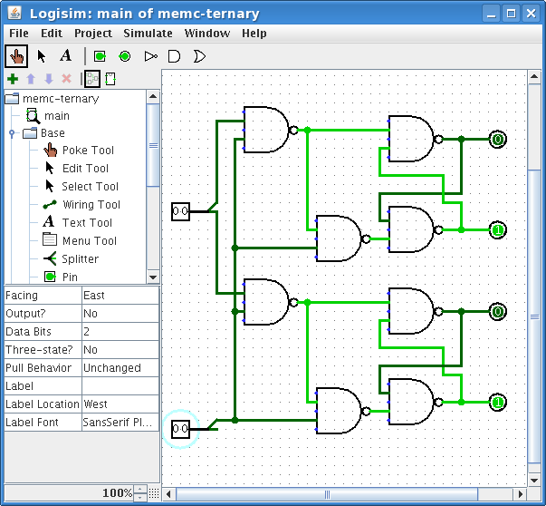
About circ-format - it is relatively easy one, because wires described as separate lines and it looks like Logisim constructs circuits from them on load. We even don't need to specify width of every wire (as 1-wire or 2-wire or more in one line) - it's just wire (but we need to specify width of every pin). Logisim builds network in moment of showing of schematics. That's cool!

What I don't like - there are bunch of lines in circ-files describing loaded libraries and some settings - so it looks like unrelated garbage for me. For example in 75 lines of simplest scheme (1 input pin directly connected to 1 output pin) only these 9 lines (12%) actually describe schematics:

Code: Select all

    <wire from="(130,170)" to="(200,170)"/>
    <comp lib="0" loc="(130,170)" name="Pin">
      <a name="tristate" val="false"/>
    </comp>
    <comp lib="0" loc="(200,170)" name="Pin">
      <a name="facing" val="west"/>
      <a name="output" val="true"/>
      <a name="labelloc" val="east"/>
    </comp>
In order to make binary coded ternary simplest scheme from this binary scheme we simply need to add

Code: Select all

<a name="width" val="2"/>
to every pin definition.

Also path to custom libraries is sometimes saved as relative, but sometimes as absolute - it is bad and inconsistent...
jay4th

Re: Jay's stuff

Post by jay4th »

I am not too surprised about the level of bloat. The author is an academic, the format is based on XML, and the language is Java. All are cultural indications that the format is going to be verbose. Nothing about any of those three (with a minor exception for XML perhaps) forces bloated representations. But still... Me? Oh, I like asn.1 and json as file formats when something simple and line oriented won't do.

About pin widths: Most of the pins in my trinary-simulator thingy are 2 bits. But there are plenty that are 12 bits since I am building 6t 'parts'.

Do you plan to make DDT output stuff for Logisim? Another set of targets to consider: SystemC, Verilog, and ... I forget the other popular HDL's name. Oh well... those guys.

Meanwhile: I've been working on eliminating the Logisim muxes from my design, reducing all the circuits to wires, and's, or's and not's. I got the adder cleaned up a few days ago. Finished the stack today. A 6t wide, 18 element deep stack is about 850 74xx chips. Looks like if I build a trinary machine I'll be faking the stacks as well as main memory with binary memory chips.
jay4th

Re: Jay's stuff

Post by jay4th »

Good news: I found the cause of the oscillation bug. Bad news: it's in the latch, one of the lowest level circuits. It has one use case where it is sensitive to glitching. I suspect all three level logic circuits (and indeed all MVL) will be sensitive to glitching in similar use cases.

The use case is this: Latching a 01 representing a 1. The problem exists both in my simulated trinary circuit, and in real implementations of the circuit in real three level signaling systems.

Suppose as the latch enable is transitioning from -1 to 1 (10 to 01), it spends long enough in the 0 state (00) for the lower left TNAND to see it. The TNAND finds the minimum of it's inputs as 0 (1 from reset, 1 from latch output, and 0 from the glitching enable). It computes the STI of the minimum, this is the definition of Trinary nand behavior. It outputs 0.

At this time the enable finishes its transition to 1. The lower left TNAND computes the minimum of it's inputs (1) and inverts it (-1) and outputs it. Meanwhile the output nand is computing the minimum of it's inputs (0 and 1), finds 0, inverts it and outputs it. In the next time period the lower left sees the 0 and passes it; the output sees the -1 and inverts it to output 1. We are in the oscillating cycle here.

The problem is a value other than the STI of the output gets onto the wire between the lower left and the output nands just before the lower left nand finishes it's state switching.

I am sure a more glitch proof design exists, I'll have to search for it. But although -1,1 is a very convenient signaling scheme, it is also very prone to introducing glitches. I'll have to come up with a design that uses 0,1 or -1,0 to signal the two states of the latch (following and remembering).

The reason this is bad news: any change in the size of the latch will be multiplied many hundreds of times in a full computer. If I get genius inspiration and actually find a smaller non-glitching latch that will be good news, but I don't expect it. The stack (a heavy user of latches) will grow past it's current 850 or so chips.
User avatar
Shaos
Admin
Posts: 24011
Joined: 08 Jan 2003 23:22
Location: Silicon Valley

Re: Jay's stuff

Post by Shaos »

What if you will use binary implementation of binary coded ternary D-latch?

Image

It is only two 74LS00. And this is version with reset (C=-1):

Image

+ 1 inverter, 1 or and two 3 input nands instead of two 2 input (approx four 74LS00).
jay4th

Re: Jay's stuff

Post by jay4th »

I am laughing because it's so obvious, and I completely didn't think of it or see it as an option. Yes, I can make that work.
User avatar
Shaos
Admin
Posts: 24011
Joined: 08 Jan 2003 23:22
Location: Silicon Valley

Re: Jay's stuff

Post by Shaos »

And this is my variant of binary coded ternary MUX:

Image

From up to bottom: N, O, P, S and on the right side - C.

In reality it could be implemented by a single 74LS153 (dual multiplexer 4:1)
jay4th

Re: Jay's stuff

Post by jay4th »

OK I understand now why I didn't consider the pair of binary triggers type solutions as a solution to a trinary trigger.

There are two similar goals that my trinary library and Logisim can be used for. 1: To explore trinary logic. 2: To design a trinary computer. At different times over the past weeks I have pursued both goals. When struggling to find a good trinary trigger I was motivated by 2, but actually pursuing goal 1.

For goal designing a trinary computer I might actually build, pragmatics wins over any 'purity' goal. Almost certainly a BCT based design will be the cheapest most easily implemented. Pursuing this goal I would favor solutions such as a pair of binary triggers to store trinary state in registers and stacks etc. Pursuing this goal I would implement a trinary stack using binary shift registers 74x299 or binary memory, I would implement trinary registers using binary ones. Only the trinary ALU might require use of SSI type 74xx chips such as NAND/AND/OR/NOR etc. Though the adder is probably best done using 4:1 mux gates. In fact once the decision to use BCT signaling is made, the right solution is probably a FPGA. There are reasons you might want to build a computer from smaller scale parts (it's much 'cooler' it seems to me, more fun). But if the goal is just a (BCT) Trinary computer, FPGA will probably be the cheapest, fastest and physically smallest solution.

For the goal of exploring trinary logic, we have to imagine that binary gates don't exist, or are too expensive to use very often. We have to imagine that the pair of 'wires' in Logisim is actually a single wire. We have to imagine that inside the trinary gates are transistors, not networks of binary gates. For this goal, I still don't have a solution for triggers. The options are a glitch prone design I came up with, or a trinary analog of the Muller C gate which almost works right and might be adapted to become a useful trigger for implementing trinary registers and stacks. I have two untested designs based on DG403's that needs to be tried (I hope to do so soon) and characterized, and then modeled in Logisim. I also have an important negative result which suggests that working with real three-level-logic gates will make glitches and hazards a much more important design issue.

There is a third possibility. Suppose your goal is to build a computer that uses mostly 3 signals per wire. This leads to DG403 type solutions. To use Logisim to help validate the design we have to, outside of a limited number of parts, pretend that the pair wires is a single wire. Inside the DG403 model in Logisim we can break the two wires apart, or perhaps the insides of the dg403 model is Java, not a Logisim network.
User avatar
Shaos
Admin
Posts: 24011
Joined: 08 Jan 2003 23:22
Location: Silicon Valley

Re: Jay's stuff

Post by Shaos »

Yes, FPGA is more appropriate for BCT, but anyway it's better to be developed and debugged in Logisim ;)
User avatar
Shaos
Admin
Posts: 24011
Joined: 08 Jan 2003 23:22
Location: Silicon Valley

Re: Jay's stuff

Post by Shaos »

This is my library with functions MUX,E12,E21,MEM and constants N,O,P:

http://www.nedopc.org/ternary/ternary_circ.zip

On the first page you can see full adder for test:

Image

P.S. It's identical to Jay's full adder but with e12/e21-multiplexers that simplified design a little

P.P.S. Constants N,O,P were added on January 5th
User avatar
Shaos
Admin
Posts: 24011
Joined: 08 Jan 2003 23:22
Location: Silicon Valley

Re: Jay's stuff

Post by Shaos »

Shaos wrote: This is my library with functions MUX,E12,E21,MEM and constants N,O,P:

http://www.nedopc.org/ternary/ternary_circ.zip

On the first page you can see full adder for test...
Last version has ternary clock (only seconds) as first page:

Image

You need to enable "Ticks" and set frequency to 8 Hz.
User avatar
Shaos
Admin
Posts: 24011
Joined: 08 Jan 2003 23:22
Location: Silicon Valley

Post by Shaos »

moving up
Я тут за главного - если что шлите мыло на me собака shaos точка net