Hi, first post here! I hope not to go OT with this...
I've bought a KR1801VM2 CPU (it is on the way...) and I'm starting just now to try to "understand" this CPU.
I've seen your work on hackaday, but I miss a complete datasheet of this IC (and no, I don't speak Russian...).
I've found a partial datasheet here: https://bitbucket.org/cfib90/1801vm2/sr ... s/1801vm2/ but a lot of pages are missing (they should be about 166 pages).
The part I'm looking for is the "sequence" and timings for the DMA request "handshaking" (#DMR, #DMGO, #SACK) and if there is a sort of "Wait" signal to accommodate slow I/O (may be #SP1 and #SP2 pins???) and its timing.
As far as I've understood up to know the I/O is memory mapped only and there are two "pages" of 64Kwords (16bit wide) selected with the #SEL signal.
This second "hidden" page seems to be used for "special" purposes with a sort of exception handling (but I haven't any detail).
Regards.
J4F
Wanting "play" with a KR1801VM2...
Moderator: Shaos
-
Just4Fun
- Writer
- Posts: 15
- Joined: 19 Oct 2020 02:55
-
Shaos

- Admin
- Posts: 24955
- Joined: 08 Jan 2003 23:22
- Location: Silicon Valley
Re: Wanting "play" with a KR1801VM2...
Actually VM2 is trying to resemble PDP-11 (more precisely LSI-11) as close as possible, so you can read PDP-11 docs 1st to see how it's supposed to work.
We have a topic with timings taken from official VM2 datasheet - see viewtopic.php?f=95&t=18777 (unfortunately it's all in Russian, so you need to use Goodle translate or something).
Basically PDP-11 doesn't have WAIT signal - all data bus communications are happening with a handshake so any peripheral must response in handshake in order data transfer to happen, so if it's slow then it simply response slower (but it can not be too slow otherwise on-board watchdog will send chip to trap).
-
Just4Fun
- Writer
- Posts: 15
- Joined: 19 Oct 2020 02:55
Re: Wanting "play" with a KR1801VM2...
Hi, thanks for the info!
Currently I'm "exploring" your forum and finding a lot of stuff. Really a gold mine!
Here I found a really explicative paper on the KR1801VM2, that made me see "the light"...
More, it seems that I can "pause" the CPU with the AR signal as explained here.
I also noticed that the SP1 and SP2 signals (pin 10 and 11) in the original scanned documentation, are commonly called as WRQ ans WAKI.
Having a fully static design will help a lot during the experiment...
Now I have to read more documentations before to decide the approach to follow for the first experiments (KR1801VM2 + MCU, KR1801VM2 + CPLD/FPGA or both...).
Regards.
-
Shaos
- Admin
- Posts: 24955
- Joined: 08 Jan 2003 23:22
- Location: Silicon Valley
Re: Wanting "play" with a KR1801VM2...
This is another project VM2+MCU that was mentioned in our mailing list:
https://github.com/jaquinn/RetroShield-KR1801VM2
Also WRQ and WAKI are window access commands for multiprocessor systems that share the same memory
WRQ - request to use window (output)
WAKI - acknowledge for window usage (input)
"Window" is part of upper memory 160000..163777 (1110 0000 0000 0000...1110 0111 1111 1111)
In my experiments I connected WAKI to ground and pull-up WRQ to +5V (in this case "window" is disabled and all memory is accessible)
-
Just4Fun
- Writer
- Posts: 15
- Joined: 19 Oct 2020 02:55
Re: Wanting "play" with a KR1801VM2...
Thanks!
That is near to the way I usually go with "legacy" 5V CPU for first experiments, using a breadboard-able custom board with the MCU + SD + serial (on USB), like I did with a V20 CPU:
I'm thinking to use the AR signal to stop the 180VM2 at the beginning of an I/O operation (I/O address space) and wait for the MCU "attention", followed by the data handshaking sequence made to accommodate the exception timeout (so from the MCU point of view this will be a time critical sw section with all the IRQ disabled; just a raw idea, I have to study this more deeply to be sure that it can be done).
It will be a "long term project" for sure...
You do not have the required permissions to view the files attached to this post.
-
Shaos
- Admin
- Posts: 24955
- Joined: 08 Jan 2003 23:22
- Location: Silicon Valley
Re: Wanting "play" with a KR1801VM2...
Cool 
Don't forget that there is "read-modify-write" cycle that is happening pretty frequently:
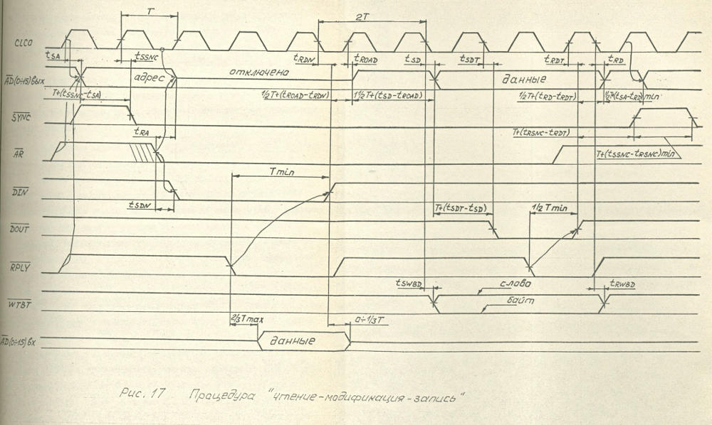
Here you have only one /AR but then read cycle and write cycle one after another for the same address
Don't forget that there is "read-modify-write" cycle that is happening pretty frequently:
Here you have only one /AR but then read cycle and write cycle one after another for the same address
-
Just4Fun
- Writer
- Posts: 15
- Joined: 19 Oct 2020 02:55
Re: Wanting "play" with a KR1801VM2...
Thanks for pointing this out...
Not sure if this "read-modify-write" cycle can be really useful in the I/O address space too, where the read/write operations are in general not "symmetrical" (reading and writing in the same address can do different things). Of course it depends on the way the I/O HW is done.
Anyway the CPU is just arrived!
Now I've to find the time... currently playing with a 68008 CPU... we'll see...
You do not have the required permissions to view the files attached to this post.
-
Shaos
- Admin
- Posts: 24955
- Joined: 08 Jan 2003 23:22
- Location: Silicon Valley
Re: Wanting "play" with a KR1801VM2...
Problem with read-modify-write cycle is it's happening very frequently even when it's not needed, so you need to make it working even for IO (that I assume mapped to usual memory address space)Just4Fun wrote:Thanks for pointing this out...
Not sure if this "read-modify-write" cycle can be really useful in the I/O address space too, where the read/write operations are in general not "symmetrical" (reading and writing in the same address can do different things). Of course it depends on the way the I/O HW is done.
-
Just4Fun
- Writer
- Posts: 15
- Joined: 19 Oct 2020 02:55
Re: Wanting "play" with a KR1801VM2...
I've resumed this thread because I'm starting now with this CPU (I've had other things in my "to do" list and now I'm ready...).
Currently I've just started to do some tests using a custom "shield" for a my development board (PIC18F based):
The first thing I want check is the real need of all the "heavy" pullups (typically 2.2k) I've seen "around", when connecting the KR1801VM2 to modern CMOS circuitry.
On the original datasheet (in Russian) the guarantied I(OH) is 200uA, so no so weak.
I've tested the CLCO output (with an 8MHz CLCI input) without any pullup and "loading" the output with a 47k resistor (to GND) so sinking about 100uA at V(OH), and result seems to be ok:
So I'm start thinking that a generic 10k pullup for the 3-state lines is adequate, and no pullup at all for the output only lines (i.e. /SEL, /WTBT, /IAKO etc.).
Just to know if someone else did this kind of test...
You do not have the required permissions to view the files attached to this post.
-
Shaos
- Admin
- Posts: 24955
- Joined: 08 Jan 2003 23:22
- Location: Silicon Valley
Re: Wanting "play" with a KR1801VM2...
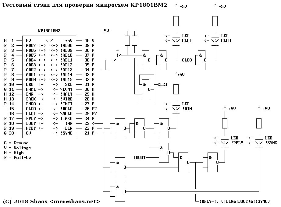
This is simplest testing schematics around VM2 that I used in 2018:
-
Just4Fun
- Writer
- Posts: 15
- Joined: 19 Oct 2020 02:55
Re: Wanting "play" with a KR1801VM2...
Ok thank you.
This is similar to what I'm doing now.
Next step will be a plug-in board for the Studio 68, a custom FPGA-centric board for retro-computing "experiments" that I've done this year.
Here the rendering of the final board:
And this is the Studio 68 board:
These two boards should be enough to implement a sort of PDP11/03, making all the I/O stuff inside the FPGA.
We'll see...
You do not have the required permissions to view the files attached to this post.
-
Just4Fun
- Writer
- Posts: 15
- Joined: 19 Oct 2020 02:55
Re: Wanting "play" with a KR1801VM2...
* UPDATE *
Unfortunately my KR1801VM2 seems to be a not working unit.
The only working pin is the CLCO output that shows the half frequency of the CLCI input (that suggested me that the CPU was working during first tests).
The other pins are dead.
Here the power on sequence with my "shied" board. Note the the /INIT pin is always at 1. It should be at 0 at the beginning when both /DCLO and /ACLO are active (at 0).
The /WAKI pin is grounded.
More, there isn't any activity on /SEL, /DIN and /SYNC pins after more than 200 CLCI clock pulses (and the same increasing the number of clock pulses).
I've done also other checks with a scope and adding 2k7 pullups on almost every pin as you did with the same result.
This is the only unit I have so I have to give up...
Unfortunately my KR1801VM2 seems to be a not working unit.
The only working pin is the CLCO output that shows the half frequency of the CLCI input (that suggested me that the CPU was working during first tests).
The other pins are dead.
Here the power on sequence with my "shied" board. Note the the /INIT pin is always at 1. It should be at 0 at the beginning when both /DCLO and /ACLO are active (at 0).
The /WAKI pin is grounded.
More, there isn't any activity on /SEL, /DIN and /SYNC pins after more than 200 CLCI clock pulses (and the same increasing the number of clock pulses).
Code: Select all
KR1801VM2 Test Shield - A140822 (PicOne A300320-R230720) - CPU Test0
CPU NOP tester

--> DCLO and ACLO set LOW
--> INIT = 1

Press the USR key to continue... --> USR key pressed

--> Done 100 clock pulses
--> INIT = 1

Press the USR key to continue... --> USR key pressed


--> DCLO set HIGH
--> INIT = 1
--> Done 100 clock pulses

--> ACLO set HIGH
--> INIT = 1

--> SEL = 1 - DIN = 1 - SYNC = 1
--> SEL = 1 - DIN = 1 - SYNC = 1
--> SEL = 1 - DIN = 1 - SYNC = 1
--> SEL = 1 - DIN = 1 - SYNC = 1
--> SEL = 1 - DIN = 1 - SYNC = 1

              <....>

--> SEL = 1 - DIN = 1 - SYNC = 1
--> SEL = 1 - DIN = 1 - SYNC = 1
--> SEL = 1 - DIN = 1 - SYNC = 1
--> SEL = 1 - DIN = 1 - SYNC = 1
--> SEL = 1 - DIN = 1 - SYNC = 1
Sent 200 clock pulses
* * * Too much clock pulses elapsed! - AbortedThis is the only unit I have so I have to give up...
-
Shaos
- Admin
- Posts: 24955
- Joined: 08 Jan 2003 23:22
- Location: Silicon Valley
Re: Wanting "play" with a KR1801VM2...
Some VM2 may not work and some may work only on pretty high frequencies (especially white ones).
Working VM2 should behave like this:
Working VM2 should behave like this:
Code: Select all
; DCLO and ACLO set to the ground
такт   1: DIN=H SYNC=L CLCO=L
такт   2: DIN=H SYNC=L CLCO=L
такт   3: DIN=H SYNC=L CLCO=L
такт   4: DIN=H SYNC=L CLCO=L
такт   5: DIN=H SYNC=L CLCO=L
; set DCLO to hight
такт   6: DIN=H SYNC=H CLCO=H
такт   7: DIN=H SYNC=H CLCO=L
такт   8: DIN=H SYNC=H CLCO=H
такт   9: DIN=H SYNC=H CLCO=L
такт  10: DIN=H SYNC=H CLCO=H
такт  11: DIN=H SYNC=H CLCO=L
такт  12: DIN=H SYNC=H CLCO=H
такт  13: DIN=H SYNC=H CLCO=L
такт  14: DIN=H SYNC=H CLCO=H
такт  15: DIN=H SYNC=H CLCO=L
такт  16: DIN=H SYNC=H CLCO=H
такт  17: DIN=H SYNC=H CLCO=L
такт  18: DIN=H SYNC=H CLCO=H
такт  19: DIN=H SYNC=H CLCO=L
; set ACLO to high
такт  20: DIN=H SYNC=H CLCO=H
такт  21: DIN=H SYNC=H CLCO=L
такт  22: DIN=H SYNC=H CLCO=H
такт  23: DIN=H SYNC=H CLCO=L
такт  24: DIN=H SYNC=H CLCO=H
такт  25: DIN=H SYNC=H CLCO=L
такт  26: DIN=H SYNC=H CLCO=H
такт  27: DIN=H SYNC=H CLCO=L
такт  28: DIN=H SYNC=H CLCO=H
такт  29: DIN=H SYNC=H CLCO=L
такт  30: DIN=L SYNC=H CLCO=H <<< read start address
такт  31: DIN=L SYNC=H CLCO=L <<< read start address
такт  32: DIN=L SYNC=H CLCO=H <<< read start address
такт  33: DIN=H SYNC=H CLCO=L
такт  34: DIN=H SYNC=H CLCO=H
такт  35: DIN=H SYNC=H CLCO=L
...
-
Just4Fun
- Writer
- Posts: 15
- Joined: 19 Oct 2020 02:55
Re: Wanting "play" with a KR1801VM2...
I've replicated exactly your sequence with the same (bad) result:
The only pin that does "something" is CLCO.
End of the story.
Code: Select all
KR1801VM2 Test Shield - A140822 (PicOne A300320-R230720) - CPU Test0
CPU NOP tester

--> DCLO and ACLO set LOW
INIT = 1

Press the USR key to continue... --> USR key pressed

--> CLCI pulse 1: SEL = 1 - DIN = 1 - SYNC = 1 - CLCO = 1
--> CLCI pulse 2: SEL = 1 - DIN = 1 - SYNC = 1 - CLCO = 0
--> CLCI pulse 3: SEL = 1 - DIN = 1 - SYNC = 1 - CLCO = 1
--> CLCI pulse 4: SEL = 1 - DIN = 1 - SYNC = 1 - CLCO = 0
--> CLCI pulse 5: SEL = 1 - DIN = 1 - SYNC = 1 - CLCO = 1
Done 5 clock pulses
INIT = 1

Press the USR key to continue... --> USR key pressed


--> DCLO set HIGH
INIT = 1
--> CLCI pulse 6: SEL = 1 - DIN = 1 - SYNC = 1 - CLCO = 0
--> CLCI pulse 7: SEL = 1 - DIN = 1 - SYNC = 1 - CLCO = 1
--> CLCI pulse 8: SEL = 1 - DIN = 1 - SYNC = 1 - CLCO = 0
--> CLCI pulse 9: SEL = 1 - DIN = 1 - SYNC = 1 - CLCO = 1
--> CLCI pulse 10: SEL = 1 - DIN = 1 - SYNC = 1 - CLCO = 0
--> CLCI pulse 11: SEL = 1 - DIN = 1 - SYNC = 1 - CLCO = 1
--> CLCI pulse 12: SEL = 1 - DIN = 1 - SYNC = 1 - CLCO = 0
--> CLCI pulse 13: SEL = 1 - DIN = 1 - SYNC = 1 - CLCO = 1
--> CLCI pulse 14: SEL = 1 - DIN = 1 - SYNC = 1 - CLCO = 0
--> CLCI pulse 15: SEL = 1 - DIN = 1 - SYNC = 1 - CLCO = 1
--> CLCI pulse 16: SEL = 1 - DIN = 1 - SYNC = 1 - CLCO = 0
--> CLCI pulse 17: SEL = 1 - DIN = 1 - SYNC = 1 - CLCO = 1
--> CLCI pulse 18: SEL = 1 - DIN = 1 - SYNC = 1 - CLCO = 0
--> CLCI pulse 19: SEL = 1 - DIN = 1 - SYNC = 1 - CLCO = 1
Done 14 clock pulses

--> ACLO set HIGH
INIT = 1

--> CLCI pulse 20: SEL = 1 - DIN = 1 - SYNC = 1 - CLCO = 0
--> CLCI pulse 21: SEL = 1 - DIN = 1 - SYNC = 1 - CLCO = 1
--> CLCI pulse 22: SEL = 1 - DIN = 1 - SYNC = 1 - CLCO = 0
--> CLCI pulse 23: SEL = 1 - DIN = 1 - SYNC = 1 - CLCO = 1
--> CLCI pulse 24: SEL = 1 - DIN = 1 - SYNC = 1 - CLCO = 0
--> CLCI pulse 25: SEL = 1 - DIN = 1 - SYNC = 1 - CLCO = 1
--> CLCI pulse 26: SEL = 1 - DIN = 1 - SYNC = 1 - CLCO = 0
--> CLCI pulse 27: SEL = 1 - DIN = 1 - SYNC = 1 - CLCO = 1
--> CLCI pulse 28: SEL = 1 - DIN = 1 - SYNC = 1 - CLCO = 0
--> CLCI pulse 29: SEL = 1 - DIN = 1 - SYNC = 1 - CLCO = 1
--> CLCI pulse 30: SEL = 1 - DIN = 1 - SYNC = 1 - CLCO = 0
--> CLCI pulse 31: SEL = 1 - DIN = 1 - SYNC = 1 - CLCO = 1
--> CLCI pulse 32: SEL = 1 - DIN = 1 - SYNC = 1 - CLCO = 0
--> CLCI pulse 33: SEL = 1 - DIN = 1 - SYNC = 1 - CLCO = 1
--> CLCI pulse 34: SEL = 1 - DIN = 1 - SYNC = 1 - CLCO = 0
--> CLCI pulse 35: SEL = 1 - DIN = 1 - SYNC = 1 - CLCO = 1
Done 16 clock pulses
* * * Too much clock pulses elapsed! - AbortedEnd of the story.
-
Shaos
- Admin
- Posts: 24955
- Joined: 08 Jan 2003 23:22
- Location: Silicon Valley
Re: Wanting "play" with a KR1801VM2...
Can you describe where you connect every pin of VM2?