В этом году это будет 4-битный ЦПУ с лампочками и кнопочками
P.S. 2 ноября 2022 года появилось ютюб-видео от автора:
Moderator: Lavr

4-bit processor simulated by 16-bit MCU. Registers, flags, ALU, SP, two Data Memory pages, current Program Word and some internal logic states are displayed in binary form, with 272 LEDs.
- A total of 31 instructions
- Processing speed: adjustable (in runtime) from 300,000 ips to 0.5 ips, plus Single Step
- Program Memory: 4096 pgm words × 12 bits
- Data Memory: 256 nibbles (32 visible in real time), including 16+6 SFRs and 10 GPRs
- 5-deep Subroutine Stack
- Instructions are 4-bit aligned, visible on 3×16 LED disassembler display
- Three ways of programming:
1. Direct, using on-board buttons in Binary or Select mode
2. Indirect, using 2-pass assembler, created by Mike Szczys
3. Save/Load to/from external file or other unit (using serial I/O) or internal flash
- Bootloader for firmware update
- I/O port with 4-bit IN and 4-bit OUT
- 3V (2×AA) Battery supply
- SAO port with Serial I/O
- Detailed User Manual
- Dimensions 17.5×9.5 cm

Эээ..Shaos wrote:На самом деле сзади спрятался PIC24, ...
Вот - самый момент состряпать стартап, нашлёпать этих бейджей и быстро удовлетворить спрос всех желающих!Shaos wrote:А вообще твиттер взорвался от этого бейджа
По словам автора, изображённая на плате принципиальная схема не совсем правильно отображает реальную работу процессора:Shaos wrote:https://hackaday.com/2022/10/12/the-2022-supercon-badge-is-a-handheld-trip-through-computing-history/
В этом году это будет 4-битный ЦПУ с лампочками и кнопочками
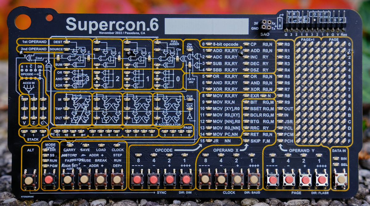
P.S. Кстати все заметили, что плата имеет 2-цветную шелкографию?The schematic is greatly simplified, good for rough reference and principles only. A much larger area would be required to represent the correct logic and, in particular, the data path. For example, not all instructions affect the state of the accumulator or flags, but the enable logic is omitted. Also, the 4-bit XOR circuit that serves as true/invert logic (below the Cout line from the adder) should not be on the DEST but on the SOURCE bus, which is not represented at all. This one would be good for SUBR instruction, but it does not exist here.
There is another formal inconsistency – there is no accumulator in the processor, but 16 selectable GP registers, which are memory mapped. Therefore, the accumulator in the schematics should be actually considered not a single register but a flexible destination, which depends on the context of the instruction. Imagine the schematics that represent the correct write logic and data path.
This is just a badge, which is too big anyway, so compromise was inevitable.
И сколько из $256 составляет цена самогО этого бейджика?Shaos wrote:Кстати все заметили, что плата имеет 2-цветную шелкографию?
Ну там много накладывают - в 2019 там даже моя платка былаLavr wrote:А заодно - что еще накладут в мешочки "с ништяками"?
Так сколько всё жеLavr wrote:И сколько из $256 составляет цена самогО этого бейджика?Shaos wrote:Кстати все заметили, что плата имеет 2-цветную шелкографию?
На сайте проекта появились архивы с исходниками прошивки на ассемблере для MPLAB X IDE, исходниками платы бейджа с герберами (вариант с упрощённой однослойной шелкографией), а также исходники макетной платы для расширения - все платы в формате CSPcbDoc ( https://en.wikipedia.org/wiki/CircuitMaker ):Shaos wrote:Автором бейджа является небезызвестный компьютерный дедушка Voja Antonic
Вот страничка проекта на hackaday.io (проект создан ещё в ноябре 2021 года):
https://hackaday.io/project/182568-badge-for-2020-supercon-years-of-lockdown