Code: Select all
Data serialization:
T0 - - - CARRY CARRY CARRY
T1 PC0 STK0 ROMD0 REGx0 RAM0 ROMD0 phi2: /RD high if needed
T2 PC1 STK1 ROMD1 REGx1 RAM1 ROMD1 ALU0
T3 PC2 STK2 ROMD2 REGx2 RAM2 ROMD2 ALU1
T4 PC3 STK3 ROMD3 REGx3 RAM3 ROMD3 ALU2
T5 PC4 STK4 ROMD4 REGx4 RAM4 ROMD4 ALU3
T6 PC5 STK5 ROMD5 REGx5 RAM5 ROMD5 ALU4
T7 PC6 STK6 ROMD6 REGx6 RAM6 ROMD6 ALU5
T8 PC7 STK7 ROMD7 REGx7 RAM7 ROMD7 ALU6
T9 PC8 STK8 ROMD8 CARRY CARRY CARRY ALU7
T10 PC9 STK9 ROMD9 - - - update RAM latch, if needed
T11 PC10 STK10 ROMD10 - - - phi1: /WR low if needed
T12 PC11 STK11 ROMD11 - - - phi2: /WR high if needed
T13 - - - - -
T14 - - - - -
T15 - - - - - - phi1: /RD low if needed
PC operations:
ph0 ph1 ph2
0 stk 2->3 stk 1->2 (pushing)
1 PC->stk 1 latch PC0
2 latch PC1
3 latch PC2
4 latch PC3
5 latch PC4
6 latch PC5
7 latch PC6
8 latch PC7
9 latch PC8
10 latch PC9
11 latch PC10
12 latch PC11, stk 1->PC (popping, for 4 bank bits)
13 stk 2->1 stk 3->2 (popping)
14 clear datalat load datalat
15
The ROM wait state generator is triggered on phi1 of T13.
The RAM wait state generator is triggered on phi1 of T15.
running the state stuff:
------------------------
ph0 latch state counter
ph1 update state counter, reset run flipflop (gated with state 15 for full cycle running)
ph2 reset S/R flipflop that gates johnson counter
instruction set key:
--------------------
n = 8 bit RAM address
w = 8 bit immediate value
a = 12 bit address
p = 8 bit IO port address
x = don't care bits
(n) = the memory at RAM address n
N.M = bit M of N
c = carry flag
| = logical OR
& = logical AND
^ = logical XOR
<< shift left
>> shift right
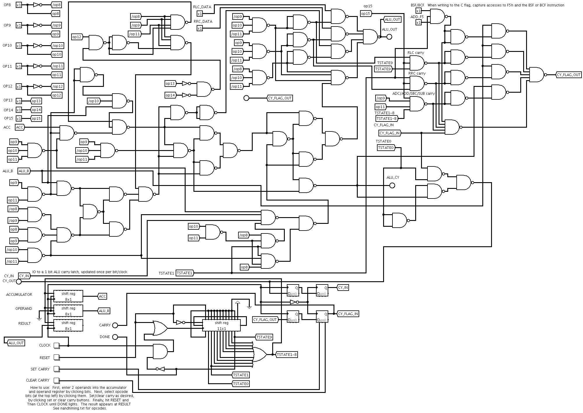
Normal ALU instructions:
------------------------
There are 6 kinds of normal ALU instructions. All work the same,
except the next instruction can be skipped depending on the state
of the zero flag.
1111 = ALU, store in F, skip if Z clear
1110 = ALU, store in A, skip if Z clear
The ALU operation is performed, then the next instruction is skipped
if the zero flag is clear.
---
1101 = ALU, store in F, skip if Z set
1100 = ALU, store in A, skip if Z set
The ALU operation is performed, then the next instruction is skipped
if the zero flag is set.
---
1011 = ALU, store in F
1010 = ALU, store in A
The ALU operation is perfomed and the next instruction is never
skipped.
???0 0000 nnnn nnnn LDA n a <- (n)
???1 0000 nnnn nnnn STA n (n) <- a
???0 0001 nnnn nnnn XOR n a <- a ^ (n)
???1 0001 nnnn nnnn XOR n,m (n) <- a ^ (n)
???0 0010 nnnn nnnn AND n a <- a & (n)
???1 0010 nnnn nnnn AND n,m (n) <- a & (n)
???0 0011 nnnn nnnn OR n a <- a | (n)
???1 0011 nnnn nnnn OR n,m (n) <- a | (n)
???0 0100 nnnn nnnn RL n a <- (n) << 1; c <- (n).7
???1 0100 nnnn nnnn RL n,m (n) <- (n) << 1; c <- (n).7
???0 0101 nnnn nnnn RLC n a <- (n) << 1 | c; c <- (n).7
???1 0101 nnnn nnnn RLC n,m (n) <- (n) << 1 | c; c <- (n).7
???0 0110 nnnn nnnn RR n a <- (n) >> 1; c <- (n).0
???1 0110 nnnn nnnn RR n,m (n) <- (n) >> 1; c <- (n).0
???0 0111 nnnn nnnn RRC n a <- (n) >> 1 | (c << 7); c <- (n).0
???1 0111 nnnn nnnn RRC n,m (n) <- (n) >> 1 | (c << 7); c <- (n).0
???0 1000 nnnn nnnn ADD n a <- a + (n); c = carry
???1 1000 nnnn nnnn ADD n,m (n) <- a + (n); c = carry
???0 1001 nnnn nnnn SUB n a <- a - (n); c = carry
???1 1001 nnnn nnnn SUB n,m (n) <- a - (n); c = carry
???0 1010 nnnn nnnn DEC n a <- (n) - 1
???1 1010 nnnn nnnn DEC n,m (n) <- (n) - 1
???0 1011 nnnn nnnn INC n a <- (n) + 1
???1 1011 nnnn nnnn INC n,m (n) <- (n) + 1
???0 1100 nnnn nnnn ADC n a <- a + (n) + c; c = carry
???1 1100 nnnn nnnn ADC n,m (n) <- a + (n) + c; c = carry
???0 1101 nnnn nnnn SBC n a <- a - (n) + c; c = carry
???1 1101 nnnn nnnn SBC n,m (n) <- a - (n) + c; c = carry
???0 1110 nnnn nnnn SETA a <- 0ffh
???1 1110 nnnn nnnn SET n (n) <- 0ffh
???0 1111 nnnn nnnn CLRA a <- 000h
???1 1111 nnnn nnnn CLR n,m (n) <- 000h
Immediate ALU instructions:
---------------------------
These instructions perform a function with the literal value, vs. a
value pulled from memory.
Depending on bit 12, a RET function is performed or not.
If bit 12 is cleared, then a return is performed along with
the ALU function. This makes it useful to perform table lookups,
index a table of offsets to add, etc. when combined with the
OFFSET instruction (see below).
The last 4 of these immediate instructions are specialized.
RET and RTI do not affect flags, or change the accumulator. RET
pops the PC off the top of stack and then adds 1 to it, while RTI
does NOT add 1. See the CALL instruction for the reasoning behind
this.
1001 = ALU, immediate
1000 = ALU, immediate, return
If the instruction returns, R is added to it like so:
LDAR #012h
XORR #034h
100? 0000 wwww wwww LDA #w a <- w
100? 0001 wwww wwww XOR #w a <- a ^ w
100? 0010 wwww wwww AND #w a <- a & w
100? 0011 wwww wwww OR #w a <- a | w
100? 0100 wwww wwww RL #w a <- w << 1
100? 0101 wwww wwww RLC #w a <- w << 1 | c; c <- w.7
100? 0110 wwww wwww RR #w a <- w >> 1 | c << 7
100? 0111 wwww wwww RRC #w a <- w >> 1 | c << 7; c <- w.0
100? 1000 wwww wwww ADD #w a <- a + w
100? 1001 wwww wwww SUB #w a <- a - w
100? 1010 wwww wwww DEC #w a <- w - 1
100? 1011 wwww wwww INC #w a <- w + 1
100? 1100 wwww wwww ADC #w a <- a + w; c = carry
100? 1101 wwww wwww SBC #w a <- a - w + c; c = carry
1000 1110 xxxx xxxx RET PC <- (top of stack) + 1
RET returns from a CALL instruction. It moves the top of stack
back into the program counter, then increments it. This is
because the following operations take place during a CALL:
0100h CALL 0200h
First, the PC is pushed onto the stack (0100h)
then address 0200h is loaded into the PC.
Next, when the RET instruction is executed, it loads the top
of stack back into the PC. The value 0100h is stored on the
stack, so 0100h would be loaded back into the PC. This would
cause the CALL instruction to be executed again. Thus, 1 is
added when it's popped so it points to 0101h, which is the
next instruction to execute.
1000 1111 xxxx xxxx RTI PC <- (top of stack)
This instruction performs similar to the RET, except it DOES NOT
add 1 to the PC when the top of stack is popped. This is due to
how interrupts work: Interrupts are performed by instruction
substitution. If the following occurs...
0100h LDA #012h
<interrupt>
0101h STA 089h
First, the LDA is executed. The interrupt input is tested at the
end of the LDA, and if an interrupt is pending, it will substitute
a JSR 008h instruction into the opcode latch, in place of the STA.
This causes the CPU to execute JSR 008h instead of STA, which pushes
the PC first, then JSR's to 008h. When the interrupt finishes,
execution should proceed back at 0101h because the STA never got
executed. Thus, 1 is NOT added to the PC so that the STA gets
executed. Otherwise, execution would pick up at 0102h which skips
the STA.
---
1001 1110 pppp pppp OUT (p) port(p) <- a
1001 1111 pppp pppp IN (p) a <- port(p)
Input or output data to IO port p.
---
0111 aaaa aaaa aaaa CALL a (top of stack) <- PC, PC <- a
The PC is first pushed to the top of stack, then it is loaded
with address a.
---
0110 aaaa aaaa aaaa JMP a PC <- a
The PC is loaded with address a.
---
0101 -bbb nnnn nnnn BTFSC x,bit if (n).b is clear, skip next instruction
0100 -bbb nnnn nnnn BTFSS x,bit if (n).b is set, skip next instruction
The memory location n is read, and then one of the 8 bits is tested.
If the bit is set or clear (depending on if BTFSC or BTFSS is run)
will determine if the next instruction is skipped.
A typical loop would look something like this:
loop: inc counter
btfss status,z
jmp loop
inc counter will increment the variable "counter", which sets the Z and N
flags depending on the result of the increment. The flags are stored
in the status register, which is mapped into RAM space.
btfss status,z is testing the zero flag. If it's set, the jmp will
be skipped over, breaking the loop. If Z is NOT set, the jmp is
executed and counter is incremented again.
jmp loop will continue the loop until it is skipped over by the btfss
instruction.
---
0011 -bbb nnnn nnnn BSF x,bit set (n).b
0010 -bbb nnnn nnnn BCF x,bit clear (n).b
These two instructions set or clear a single bit of memory in RAM.
---
0001 001x nnnn nnnn OFFSET x PC <- PC + (n) + 1
The offset instruction is how table lookups are performed. The value
of memory pointed to by n will be added to the program counter,
unsigned. This allows a lookup table that is up to 256 bytes deep.
The method works like this:
<code>
CALL tablelut
<more code>
...
tablelut:
OFFSET address
LDAR #12h
LDAR #34h
LDAR #56h
LDAR #78h
if (address) is equal to 00h, nothing is added, and execution falls through
to the LDAR #12h instruction. If (address) equals 01h, then 1 is added
to the PC, and then PC is incremented. This then points PC to the LDAR #34h
instruction, and so on.
---
All other instructions act as NOPs. 0000 0000 0000 0000 is the prototypical
NOP.
Memory accessing:
-----------------
The 8 bit address space looks like this:
00-EF : general purpose RAM
F0-F3 : not used at the moment (for inputs though)
F4 : accumulator
F5 : status register (flags)
F6 : index data port 0
F7 : index data port 1
F8-F9 : not used at the moment (for more write registers)
FA : ROM bank
FB : general RAM bank # (bits 0-3) and interrupt enable (bit 7)
FC : index register 0
FD : index bank 0
FE : index register 1
FF : index bank 1
Addresses 00-EFh simply map to RAM bytes. The 4 bit bank value is stored
at address FBh. So, to read a byte of memory located at 0123h in RAM,
the following is used:
LDA #01h ;bank 1
STA 0FBh ;(labelled "genbank")
LDA 023h ;data at addres 0123h
Addresses F0-FF always SET the 4 bank bits when accessed, so that the
value is always written to FF0-FFFh (in RAM space). This prevents
overwriting F0-FF in the bank that is currently selected.
Addresses at F0-F7 are typically input only, and cannot be written to
with the exception of the accumulator (F4h) and the status register (F5h).
The exception to this is addresses F6 and F7, which are the two index
data ports.
Index registers:
There are two index registers, IX0 and IX1. These are 8 bit registers
with 4 bit bank select registers that can be used to access a byte of
RAM indirectly. The value on IX0 and its associated bank register is
used as the address when location F6 is either read or written, likewise
IX1 and its associated bank register is used as the address when
location F7 is read or written.
The two index registers are provided to allow for copying of data, and
for processing of data in a linear fashion.