4-bit Системы команд

4-битные микроконтроллеры и микропроцессоры (прошлое, настоящее, будущее)

Moderator: Lavr

User avatar
Lavr
Supreme God
Posts: 16682
Joined: 21 Oct 2009 08:08
Location: Россия

4-bit Системы команд

Post by Lavr »

4-bit Системы команд

Размещаю здесь для обсуждения системы команд 4-битных самодельных ЦПУ, популярных в сети.
Первая - от восьмиразрядного, но автор использовал только старший ниббл.

Titan - The 8 bit TTL Processor
http://marc.cleave.me.uk/cpu/index.htm

Code: Select all

Registers:

0000    Z(Hardwired zero)
0001    Accumulator
0010    B register
0011    C register
0100    D register
0101    E register
0110    F register
0111    G register
1000    H register
1001    I register
1010    J register
1011    K register
1100    L register
1101    M register
1110    N register
1111    O register

Code: Select all

Binary		Hex	Mnenomic	Operation Excuted
0000 0000	0x00	NOP	No operation
0001 0000	0x10	ADD	Sum of the A and B registers
0010 0000	0x20	SUB	The subtraction of the B register from the A register
0011 0000	0x30	AND	Logical AND of the A and B registers
0100 0000	0x10	OR	Logical OR of the A and B registers
0101 0000	0x50	NOT	Logical NOT of the A register
0110 0000	0x60	XOR	Logical XOR of the A and B registers
0111 XXXX	0x70	PSH	Pushes the selected register onto the stack
1000 XXXX	0x80	POP	Pops the top of the stack into the selected register
1001 0000	0x90	JMP	Jumps to address
1010 0000	0xA0	JPI	Indirect jump, point to a location in memory and jumps 
to the value stored in the address
1011 0000	0xB0	JPZ	Jumps if the zero flag is set
1100 0000	0xC0	JPC	Jumps if the carry flag is set
1101 0000	0xD0	JPS	Jumps if the sign flag is set
1110 0000	0xE0	STM	Writes accumulator register to memory address
1111 0000	0xF0	LDM	Loads memory address to accumulator
Viktor's Amazing 4-bit Processor
http://www.vttoth.com/vicproc.htm

Code: Select all

Characteristics of 4-bit experimental processor:
Data bus				4 bits
Address bus				8 bits
Memory					256 4-bit word
Accumulator				8 bits
Program counter			8 bits
Data address register (internal)	8 bits
Instruction register (internal)	4 bits
Flags	Carry, Zero, Data (external I/O)
Instruction set	16 variable length instructions
The 16 machine instructions are as follows:

Code: Select all

Opcode	Mnem. Size	Description
0	HLT	1	Halts the processor. Can be restarted manually by pressing a button.
1	LDA nn	3	Load 8-bit value from address nn into AC
2	STA nn	3	Store AC at address nn.
3	JMP nn	3	Continue execution at (i.e., set PC to) address nn.
4	SPC nn	3	Store current PC value at address nn.
5	AND nn	3	Compute logical AND of AC and nn, store result in AC. Set Z flag as 
appropriate.
6	OR nn	3	Compute logical OR of AC and nn, store result in AC. Set Z flag as 
appropriate.
7	ADD nn	3	Compute arithmetic sum of AC and nn, store result in AC. Set C and Z 
flags as appropriate.
8	SUB nn	3	Subtract nn from AC, store result in AC. Set C and Z flags as 
appropriate.
9	JNZ nn	3	Jump conditional; execute JMP nn if Z flag is not set.
A	CMP nn	3	Subtract nn from AC, discard result. Set C and Z flags as appropriate.
B	JND nn	3	Jump conditional; execute JMP nn if D flag is not set.
C	JNC nn	3	Jump conditional; execute JMP nn if C flag is not set.
D	ROL	1	Rotate AC left. Move C to least significant bit of AC. Move most 
significant bit to C.
E	ROR	1	Rotate AC right. Move C to most significant bit of AC. Move least 
significant bit to C.
F	CLF	1	Clear flags C, D, and Z.
Galactic Electronics Projects - 4 bit CPU
http://www.galacticelectronics.com/Simple4BitCPU.HTML

Below is a summary of the available instructions:

Code: Select all

Code	Mnem.	Description 
1 	LIT 	Copy a literal value from program memory to the accumulator. 
2 	LOAD 	Copy a value from a register to the accumulator. 
3 	STORE 	Copy the value in the accumulator to a register. 
4 	INC 	Increment the accumulator by one. 
5 	DEC 	Decrement the accumulator by one. 
6 	REG 	Copy the value in the accumulator to the register address latch. 
7 	CMPL 	Compare the accumulator to a literal value. Sets flags. 
8 	CMPR 	Compare the accumulator to a register. Sets flags. 
9 	RST 	Resets the program counter. 
10 	JUMPL 	Copy the value in the accumulator to the segment register when the less 
than flag is set. 
11 	JUMPE 	Copy the value in the accumulator to the segment register when the 
equal flag is set. 
12 	JUMPG 	Copy the value in the accumulator to the segment register when the 
greater than flag is set. 
13 	IN 	Copy the value from the input to the accumulator. 
14 	OUT 	Copy the value in the accumulator to the output latch. 
15 	NOP 	No operation. 
As you can see, there are 15 instructions shown here instead of 16. One other instruction, FETCH, is used by the micro-instruction logic and should never be used by a program.

Gakken GMC-4
http://www.jambell.com/GMC-4/

The GMC-4 understands about 30 instructions. Of these, 15 are accessed using a single hex value and the remainder are accessed by prefixing a hex value with hex E (i.e. E0 - EF)

Program code table:

Code: Select all

Code	Mnem.	Action	Result	Flag	Detail
0	KA	K->Ar	0, 1	The pressed key from the hex keypad is saved to the A register. If a 
key is not pressed, the Flag is set to 1, otherwise it is 0.
1	AO	Ar->Op	1	The 7-segment readout displays the value currently contained in the 
A register.
2	CH	Ar<=>Br 
Yr<=>Zr	1	Exchange the contents of the A and B registers, and the Y and 
Z registers.
3	CY	Ar<=>Yr	1	Exchange the contents of the A and Y registers.
4	AM	Ar->M	1	Write the contents of the A register to data memory (memory address 
is 50 + Y register).
5	MA	M->Ar	1	Write the contents of data memory (50 + Y register) to the A 
register.
6	M+	M+Ar->Ar	0, 1	Add the contents of data memory (50 + Y register) to the A 
register. If there is overflow, the Flag is set to 1, otherwise 0.
7	M-	M-Ar->Ar	0, 1	Subtract the contents of data memory (50 + Y register) from 
the A register. If the result is negative, the Flag is set to 
1, otherwise 0.
8	TIA [ ]	[ ] -> Ar	1	Transfer immediate to the A register.
9	AIA [ ]	Ar + [ ] -> Ar	0, 1	Add immediate to the A register. If there is overflow, the 
Flag is set to 1, otherwise 0.
A	TIY [ ]	[ ] -> Yr	1	Transfer immediate to the Y register.
B	AIY [ ]	Yr + [ ] -> Yr	0, 1	Add immediate to the Y register. If there is overflow, the 
Flag is set to 1, otherwise 0.
C	CIA [ ]	Ar != [ ] ?	0, 1	Compare immediate to the A register. If equal, Flag reset to 
0, otherwise set to 1.
D	CIY [ ]	Yr != [ ] ?	0, 1	Compare immediate to the Y register. If equal, Flag reset to 
0, otherwise set to 1.
E	---	---	---		Extended code. See table below.
F	JUMP [ ] [ ]		1	Jump to the immediate address if the Flag is 1, otherwise 
just increment the program counter. The Flag is then set to 
1. Note that this is an absolute address. That is, JUMP [0] 
[2] will change the address pointer to hex address 0x02. You 
can jump both forward and backward in program space.
Extended code table.:

Code: Select all

E0	CAL RSTO	1	Clear the 7-segment readout.
E1	CAL SETR	1	Turn on the 2-pin LED using the Y register (Y register takes the 
value of 0-6).
E2	CAL RSTR	1	Turn off the 2-pin LED using the Y register (Y register takes the 
value of 0-6).
E3	---	---		Not used.
E4	CAL CMPL	1	Complement the A register (1 <=> 0).
E5	CAL CHNG	1	Swap the A/B/Y/Z registers with A'/B'/Y'/Z'
E6	CAL SIFT	0, 1	Shift the A register right 1 bit. If the starting value is even (bit 
0 = 0), set the Flag to 1, otherwise 0.
E7	CAL ENDS	1	Play the End sound.
E8	CAL ERRS	1	Play the Error sound.
E9	CAL SHTS	1	Play a short "pi" sound.
EA	CAL LONS	1	Play a longer "pi-" sound.
EB	CAL SUND	1	Play a note based on the value of the A register (allowed values are 
1 - E).
EC	CAL TIMR	1	Pause for the time calculated by (value of A register +1) * 0.1 
seconds.
ED	CAL DSPR	1	Set the 2-pin LEDs with the value from data memory. The data to 
display is as follows: the upper three bits come from memory address 
5F (bits 0-2), and the lower four from memory address 5E (bits 0-3).
EE	CAL DEM-	1	Subtract the value of the A register from the value in data memory. 
The new value is stored in data memory as a decimal. Afterwards, the 
Y register is decremented by 1.
EF	CAL DEM+	1	Add the value of the A register to the value in data memory. The new 
value is stored in memory as a decimal. If the result is overflow, 
data memory will be automatically adjusted. Afterwards, the Y 
register is decremented.
4-bit DUO 128 Elite
http://web.mac.com/teisenmann/iWeb/elit ... ecode.html

Code: Select all

Code	Mnem.	Description 

0000 - EQUAL (number) (number)
If the arguments are equal, then the boolean bit is set to 1; else, it is set to 0.
0001 - UNEQUAL (number) (number)
If the arguments are equal, then the boolean bit is set to 0; else, it is set to 1.
0010 - GREATER (number) (number)
If the first argument is greater than the second argument, then the boolean bit is set to 1; else, it is set to 0.
0011 - GOTO (address) (address)
Skips command execution to the given address.
0100 - WRITE (data) (destination)
Writes data to the given location in RAM.
0111 - INPUT (device input address) (destination)
Outputs the device input address and writes the device input at the given RAM address.
1000 - OUTPUT (data) (data) (device output address)
Writes the data at the given device output address.
1100 - ADD (number) (number) (destination)
Adds the numbers and stores the result in the given RAM address.
1101 - BITON (nybble) (bit address) (destination)
Sets the bit at the address in the nybble to 1, then stores the result in the given RAM address. Note: the digit addresses are ordered from most significant to least significant.
1110 - BITOFF (nybble) (bit address) (destination)
Sets the bit at the address in the nybble to 0, then stores the result in the given RAM address.
1111 - BITGET (nybble) (bit address) (destination)
Retrieves the bit at the address in the nybble, then stores the bit in the given RAM address.
Если у кого есть материалы и ссылки на другие интересные системы - размещение
их здесь - приветствуется.
User avatar
Lavr
Supreme God
Posts: 16682
Joined: 21 Oct 2009 08:08
Location: Россия

Post by Lavr »

Simplex-III
http://members.iinet.net.au/~daveb/simplex/simplex.html

Registers

Symbol Function Length

Code: Select all

A	Accumulator	1..8 bytes 
X1	Address base	2 bytes
X2	Address base	2 bytes
X3	Address base	2 bytes
S	Instruction counter	2 bytes
C	Condition codes/flags	8 bits
Instruction Format

Code: Select all

Operation	4 bits
Index register	2 bits
Operand register	2 bits
Instructions

Code: Select all

Definitions:
z	Content of object Z (register or memory)
Ro	The operand register (A, X1, X2, X3)
Rx	The index register (S, X1, X2, X3)
Q	The effective memory operand address, defined as (rx + l)
q	Content of Q
Where the target of an operation is shown as z, c this means the C (condition) bits are affected, as well as loading a result into z.

The instruction assignments are as follows:

Code: Select all

Code	Mnemonic	Function	Notes
0	ADD 	ro + q => ro, c 	 
1	ST 	ro => q 	 
2	LD 	q => ro, c 	 
3	XOR 	ro XOR q => ro, c	 
4	AND 	ro AND q => ro, c	 
5	LCP 	ro AND q => c 	ie as 8086 TEST instruction
6	ADS 	ro + q => q, c 	 
7	SUB 	ro - q => ro, c 	 
8	CMP 	ro - q => c 	 
9	JI/JIL	q => s 	See below for side effects
A	CTS 	q + 1 => q, c 	Always 1-byte operand only
B	SET 	  	Set values for operand length, interrupt terminate, etc.
C	RTL 	ro + ro => ro, c 	Add to itself, ie shift left
D	BC 	s +/- l => s 	Direction, and condition set by Ro, Ri bits
E	LDI 	l => ro, c 	 
F	MIR 	ro + l => rx, c 	NB Effectively moves Ro to Rx
Side effects of the JI/JIL instruction. If Ro=X1, X2, or X3, store S in Ro (ie save subroutine link). Then or otherwise, q => s (indirect jump). If this instruction is executed in interrupt level, BOTH S registers are loaded.

Home-Built TTL CPU
http://cpuville.com/

Home-Built TTL CPU is a 16-bit instruction word width. With 16 instructions, this means a 4-bit operation code, and a 12-bit operand:

Code: Select all

Opcode	Instruction Mnemonic	Operation Performed
0	ADD	Adds contents of memory to accumulator
1	ADC	Adds contents of memory and carry to accumulator
2	SUB	Subtracts contents of memory from accumulator
3	SBC	Subtracts contents of memory and complemented carry from accumulator
4	AND	Binary AND of memory with accumulator
5	OR	Binary OR of memory with accumulator
6	XOR	Binary XOR of memory with accumulator
7	NOT	Complements accumulator (operand ignored)
8	LDI	Loads 12-bit value of operand into accumulator (immediate load)
9	LDM	Loads contents of memory into accumulator
A	STM	Stores contents of accumulator to memory
B	JMP	Jumps to memory location
C	JPI	Jumps to contents of memory location (indirect jump)
D	JPZ	If accumulator = zero, jumps to memory location
E	JPM	If accumulator is negative (minus), jumps to memory location
F	JPC	If carry flag is set, jumps to memory location
User avatar
Lavr
Supreme God
Posts: 16682
Joined: 21 Oct 2009 08:08
Location: Россия

4-битная система команд

Post by Lavr »

В 4-битной системе у нас есть следующие воможности:
16 команд - мы решили было, что такой набор нас функционально не устроит.

Но VituZz внёс следующее предложение:

Code: Select all

По системе команд (если ограничиться 16-ю командами): 
0 - MOV A, M - скопировать аккумулятор в память 
1 - MOV M, A - скопировать в аккумулятор из памяти 
2 - ADD A, M - сложить аккумулятор с памятью 
3 - SUB A, M - вычесть из аккумулятора память 
5 - OR A, M - A=A И M 
4 - AND A, M - A=A ИЛИ M 
6 - JNZ M - перейти, если не равно 0 
7 - JNC M - перейти, если нет переноса 
8 - JMP M - перейти 
9 - RLC - сдвинуть влево по кольцу, C в кольце 
A - RAL - сдвинуть влево по кольцу, C не в кольце 
B - CALL M - вызвать ПП 
C - RET - вернуться 
D - PUSH A - A в стек 
E - POP A - из стека в A 
F - NOP - Нет операции 
M здесь может быть как абсолютный адрес, так и относительный; второе мне кажется предпочтительней.
31 команда (с одним префиксом).
46 команд (с двумя префиксами).
В качестве префиксов удобно использовать 0EH, 0FH.

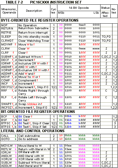
Добавлю здесь для сравнения ещё и систему команд PIC.

Image

И предлагаю определится с системой команд для 4-бит CPU.

Мне лично не хватает PUSH и POP, но при коротком стеке и большом наборе
регистров общего назначения без них обойтись можно, хотя и неудобно...

PS. У PIC-а странное вычтание: аккумулятор из аргумента, а не наоборот, как обычно привыкли...

PPS. Адресацию сразу предлагаю абсолютной, относительная сразу предполагает сумматор с РС.
User avatar
Lavr
Supreme God
Posts: 16682
Joined: 21 Oct 2009 08:08
Location: Россия

Post by Lavr »

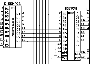
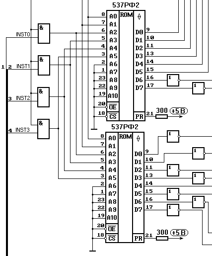
В принципе даже схемотехника прототипа даёт нам возможность сделать
инструкции 8-битными:

Image
ОЗУ инструкций


Image
ПЗУ микрокоманд
b2m
Devil
Posts: 907
Joined: 26 May 2003 06:57

Post by b2m »

На соседнем форуме делают эмуляцию дисплея 15ИЭ-00-013, который использовался с компьютерами ДВК, ДВК-2. Мне показалось, что система команд процессора этого дисплея тоже подходит под понятие 4-х битной:

Code: Select all

Binary             Mnenomic     Operation Excuted
0000rrrr           ADD  R       Add to Acc
0001xxxx xxxxxxxx  JMP  addr    Jmp to addr
0010rrrr xxxxxxxx  LDC  R,byte  Load Const
00110000 xxxxxxxx  LCA  byte    Load Const in Acc
00110011           RAL          Rotate Acc Left
00110101           RAR          Rotate Acc Right
0100rrrr           DSR  R       Decrement Reg, Skip next Cmd if = -1
01010000           ISN          Increment Acc, Skip next Cmd if = -1
01010001           INC          Increment Acc
01010010           DSN          Decrement Acc, Skip next Cmd if = -1
01011000           ISE          Increment Acc, Skip next Cmd if <> -1
01011010           DSE          Decrement Acc, Skip next Cmd if <> -1
01011011           DEC          Decrement Acc
01011101           COM          Complement Acc
01011111           CLR          Clear Acc
0110pppp           LIA  port    Load In Acc from Port
0111rrrr           JMI  R       Jmp Indexed (PC<-R)
10000fff           SFC  flag    Skip if Flag Clear
10000111           SKP          Skip
10001fff           SFS  flag    Skip if Flag Set
10001111           NOP          No Operation
1001rrrr           AND  R       And with Acc
1010rrrr           XOR  R       Xor with Acc
1011rrrr           CS   R       Compare with Acc
11000fff           CFL  flag    Clear Flag
11001fff           SFL  flag    Set Flag
1101rrrr           LDA  R       Load Acc from Reg
1110rrrr           STA  R       Store Acc to Reg
1111pppp           OTA  port    Out Acc into Port
Есть и схема этого дисплея.

Структура системы больше похожа на гарвардскую, т.к. в адресном пространстве процессора только ПЗУ программы. ОЗУ дисплея внешнее, с доступом через порты. А для программы вообще нет ОЗУ, но есть 32 регистра общего назначения, организованные в 2 банка по 16.

Помнится Lavr интересовался, как ему сделать возврат из п/п. Так вот тут сделано, я считаю, достаточно оригинально. Несмотря на то, что АЛУ и акк. у него восьмибитные, регистры тут 12-ти битные, как и счётчик команд. А команда загрузки регистра 8-ми битной константой записывает старшие 4 бита регистра из старших 4-х бит PC. Эти старшие 4 бита регистра используются только в команде JMI.

Таким образом, перед вызовом п/п мы записываем в регистр адрес возврата и переходим на п/п. А возврат осуществляется переходом на адрес в регистре. Что-то подобное и мы обсуждали.

Ещё тут используется пропуск следующей команды в зависимости от условия, как в некоторых микроконтроллерах.
Страничка эмулятора наших компьютеров
http://bashkiria-2m.narod.ru/
User avatar
Shaos
Admin
Posts: 24033
Joined: 08 Jan 2003 23:22
Location: Silicon Valley

Post by Shaos »

в пиках вроде бы так и сделаны дальние переходы
Я тут за главного - если что шлите мыло на me собака shaos точка net
User avatar
Lavr
Supreme God
Posts: 16682
Joined: 21 Oct 2009 08:08
Location: Россия

Post by Lavr »

b2m wrote:Помнится Lavr интересовался, как ему сделать возврат из п/п. Так вот тут сделано, я считаю, достаточно оригинально. Несмотря на то, что АЛУ и акк. у него восьмибитные, регистры тут 12-ти битные, как и счётчик команд. А команда загрузки регистра 8-ми битной константой записывает старшие 4 бита регистра из старших 4-х бит PC. Эти старшие 4 бита регистра используются только в команде JMI.

Таким образом, перед вызовом п/п мы записываем в регистр адрес возврата и переходим на п/п. А возврат осуществляется переходом на адрес в регистре. Что-то подобное и мы обсуждали.
Вопрос с возвратом из п.п., как мне показалось, я довольно скромно аппаратно разрешил
для своего поделия...
Но я остался совершенно недоволен индексным доступом. А это, собственно, весьма
важный механизм для той цели, с которой я затеял конструирование своего 4-битника.

И тут мне повернулась под руку вся обширная информация по 6502, которому я ранее
совершенно внимания не уделял.
Поэтому я и занялся сейчас им, поскольку с индексными способами в нём - богато! :o
И неожиданно 6502 показался мне очень интересным! В нём заложен минимализм,
к которому я схемотехнически стремлюсь.

Но сейчас меня всё подталкивает к отказу от жесткого числа тактов, в команде, как у меня
было изначально запланированно...

Но я на это никак решиться не могу, поскольку это хоть и упрощает микрокод, но снова
ведёт к аппаратному усложнению вокруг ПЗУ микрокоманд.

Многопараметровая и сильно взаимосвязанная вещь - конструкция процессора получается...
В одном месте - сэкономишь, в другом всё распухнет. :(

Вон я тут задал вопрос итальянцу про размер его программного счетчика - так он
руками замахал - 256 байт ему типа хватает на всё - про всё...
Понятно... даже глядя в 6502, - двумя половинками РС по 4 бита управляться легче,
нежели тремя 4-битными частями РС.

Но у 6502 я хочу как-то позаимствовать главное: раз уж я заложился в конструкции
на 4096 байт ОЗУ - вот его и надо использовать во всю ширь, а не добавлять регистры.
Конечно это прийдется продумать не раз, но есть в идеологии 6502 некая
подкупающая простота. Хотя после Интела он кажется странным... :-?
Наверное, выросшим на 6502 Интел кажется громоздким и неуклюжим... :wink:
iLavr