In January 2015 I was playing with LTspice IV and decided to create a number of reusable blocks of CMOS logic for our nedoPC.org community.
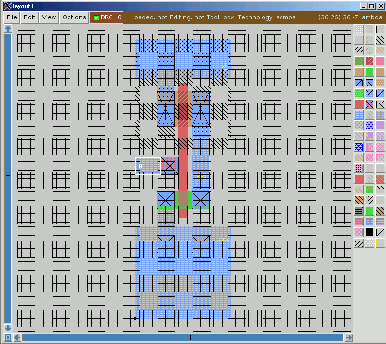
Later I started adding CMOS layouts, created in Magic VLSI Layout Tool v8.0, and some were even silicon proven in October 2015 for CMOS 0.5um technology...
http://nedopc.org/nedopc/files/nedocon-cmoslib.zip (693K) v1.0alpha (March 2016)
This PUBLIC DOMAIN archive consists of a number of close to reality
CMOS blocks for LTspice IV in form of ASC and ASY files that you need
to copy (from "sym" subfolder) to
C:\Program Files\LTC\LTspiceIV\lib\sym\
You can see internals of any block and you can use it anywhere.
Tests are also included with screenshots of oscillograms. Enjoy!
cmos-not - NOT gate (invertor)
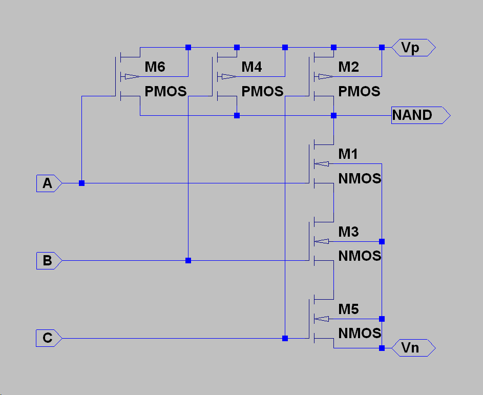
cmos-nand - 2-input NOT-AND gate
cmos-nand3 - 3-input NOT-AND gate
cmos-nor - 2-input NOT-OR gate
cmos-nor3 - 3-input NOT-OR gate
cmos-tgate - transmission gate (SPST switch)
cmos-tgate2 - 2 transmission gates connected as SPDT switch
Then it will be xor, nor-and, rs-trig, d-trig, mux2, mux4, mux8 etc.
P.S. Used book:
Uyemura, John P. Circuit design for CMOS VLSI. 1992 (11th printing 1998) ISBN 0-7923-9184-5
P.P.S. On January 8th, 2016 I started adding silicon proven Magic layouts here...
Open source CMOS reusable blocks for LTspice IV and Magic 8
Moderator: Shaos
-
Shaos

- Admin
- Posts: 25227
- Joined: 08 Jan 2003 23:22
- Location: Silicon Valley
Open source CMOS reusable blocks for LTspice IV and Magic 8
Last edited by Shaos on 16 Feb 2015 01:05, edited 14 times in total.
-
Shaos
- Admin
- Posts: 25227
- Joined: 08 Jan 2003 23:22
- Location: Silicon Valley
cmos-not
Inverter cmos-not (with added parasitic capacitor on output to simulate gate delay - about 0.1ns):
Testing:
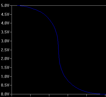
Voltage transfer curve:
P.S. In January 2016 CMOS layout 0.5um for Magic v8.0 was added here (silicon proven in October 2015):
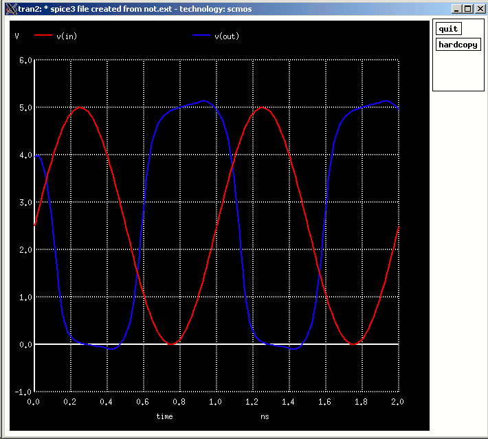
Simulation of 1 GHz input (SPICE model extracted from layout by Magic and simulated by ngspice):
 |
Testing:
 |
Voltage transfer curve:
P.S. In January 2016 CMOS layout 0.5um for Magic v8.0 was added here (silicon proven in October 2015):
 |
Simulation of 1 GHz input (SPICE model extracted from layout by Magic and simulated by ngspice):
 |
Last edited by Shaos on 04 Feb 2015 07:32, edited 2 times in total.
-
Shaos
- Admin
- Posts: 25227
- Joined: 08 Jan 2003 23:22
- Location: Silicon Valley
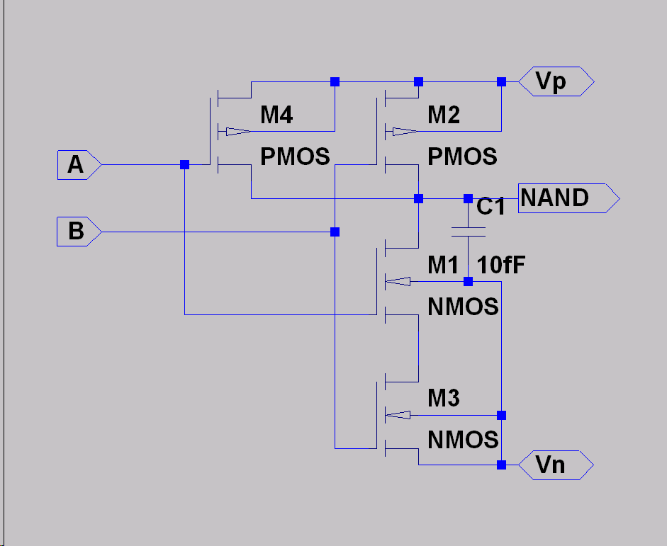
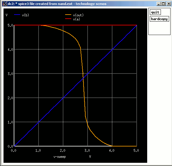
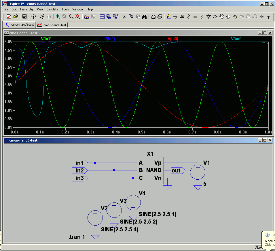
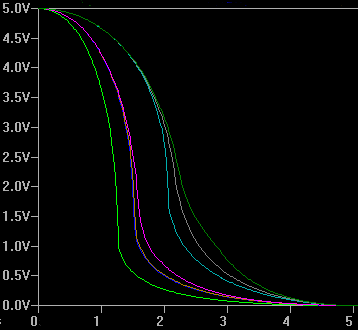
cmos-nand
Two input NAND block cmos-nand (with parasitic capacitor on output to simulate gate delay - about 0.2ns):
Test schematics:
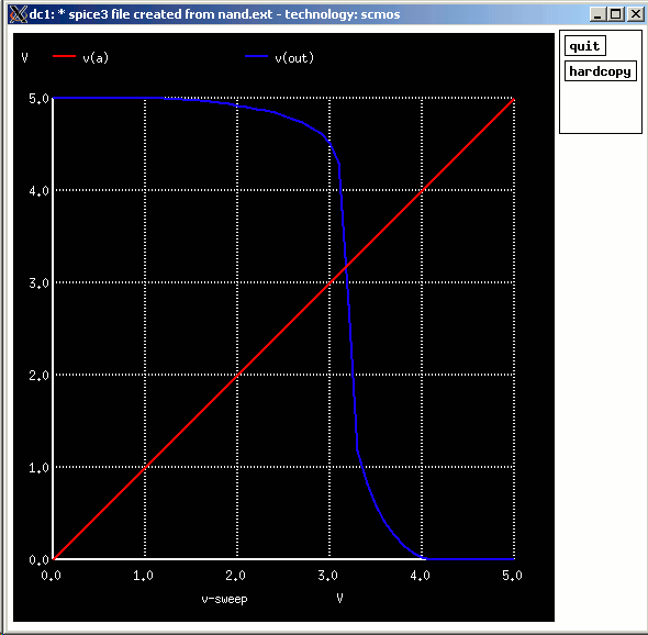
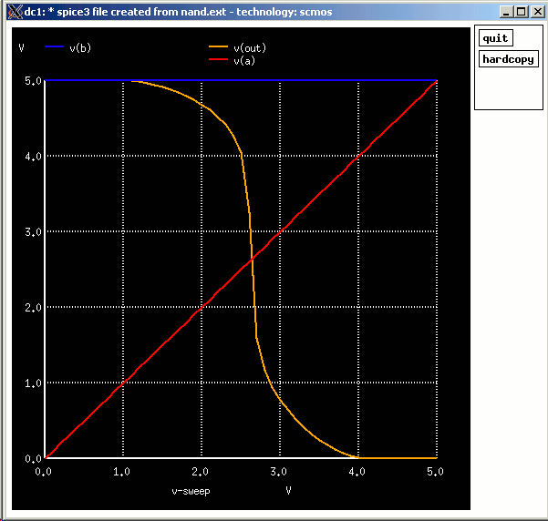
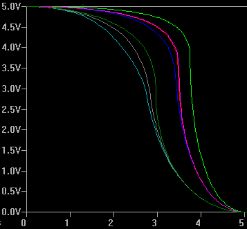
Voltage transfer curve:
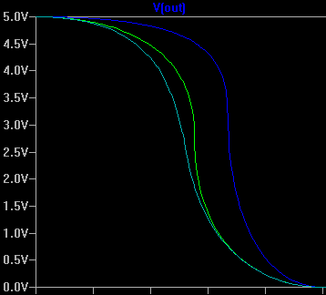
Blue curve is output when both inputs connected together and two other curves for cases when one of the inputs tied to high voltage.
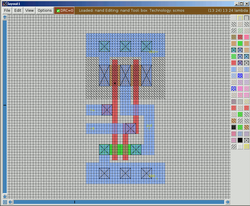
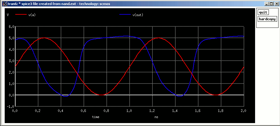
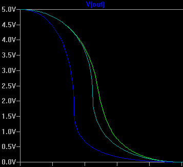
P.S. Magic layout and simulation (silicon proven in October 2015):
Both inputs changed, then just one - 1st one (A) and 2nd one (B):
1GHz signal on both inputs:
 |
Test schematics:
 |
Voltage transfer curve:
Blue curve is output when both inputs connected together and two other curves for cases when one of the inputs tied to high voltage.
P.S. Magic layout and simulation (silicon proven in October 2015):
 |
Both inputs changed, then just one - 1st one (A) and 2nd one (B):
 |
 |
 |
1GHz signal on both inputs:
 |
Last edited by Shaos on 07 Feb 2015 04:26, edited 4 times in total.
-
Shaos
- Admin
- Posts: 25227
- Joined: 08 Jan 2003 23:22
- Location: Silicon Valley
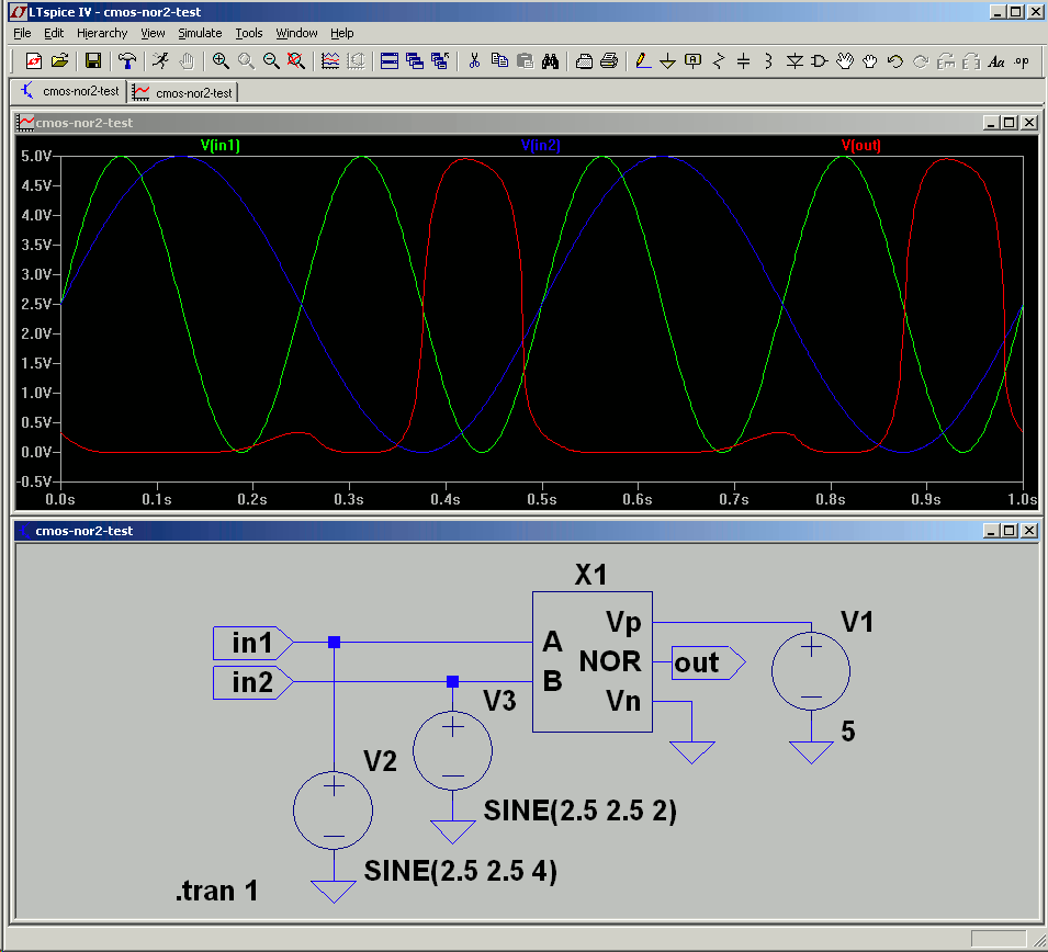
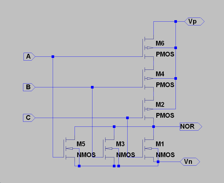
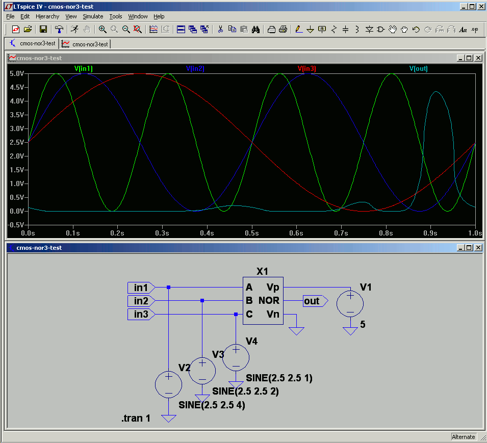
cmos-nor2
Two input NOR cmos-nor
Test schematics:
Voltage transfer curve:
Blue curve is output when both inputs connected together and two other curves for cases when one of the inputs tied to the ground.
 |
Test schematics:
 |
Voltage transfer curve:
Blue curve is output when both inputs connected together and two other curves for cases when one of the inputs tied to the ground.
Last edited by Shaos on 07 Feb 2015 04:27, edited 2 times in total.
-
Shaos
- Admin
- Posts: 25227
- Joined: 08 Jan 2003 23:22
- Location: Silicon Valley
cmos-tgate
Single CMOS switch (transmission gate) cmos-tgate
 |
 |
Last edited by Shaos on 30 Jan 2015 19:51, edited 1 time in total.
-
Shaos
- Admin
- Posts: 25227
- Joined: 08 Jan 2003 23:22
- Location: Silicon Valley
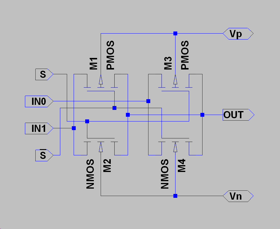
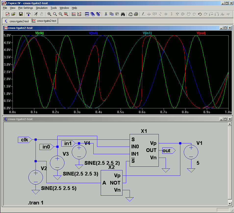
cmos-tgate2
SPDT CMOS-switch (2 transmission gates) cmos-tgate2
 |
 |
Last edited by Shaos on 30 Jan 2015 19:52, edited 1 time in total.
-
Shaos
- Admin
- Posts: 25227
- Joined: 08 Jan 2003 23:22
- Location: Silicon Valley
Re: CMOS reusable blocks for LTspice IV (PUBLIC DOMAIN)
I moved library elements to folder "sym"
-
Shaos
- Admin
- Posts: 25227
- Joined: 08 Jan 2003 23:22
- Location: Silicon Valley
Re: Open source CMOS reusable blocks for LTspice IV and Magi
I decided to add "silicon proven" layouts of CMOS reusable blocks to the same archive...
-
Shaos
- Admin
- Posts: 25227
- Joined: 08 Jan 2003 23:22
- Location: Silicon Valley